-
E-mail
frank.yang@acuitik.com
-
Phone
13817395811
-
Address
4th Floor, No. 298 Xiangke Road, Pudong New Area, Shanghai
Product Categories
Suzhou Xishi Technology Co., Ltd
Film thickness measurement kit
NegotiableUpdate on 02/09
- Model
- Nature of the Manufacturer
- Producers
- Product Category
- Place of Origin
Overview
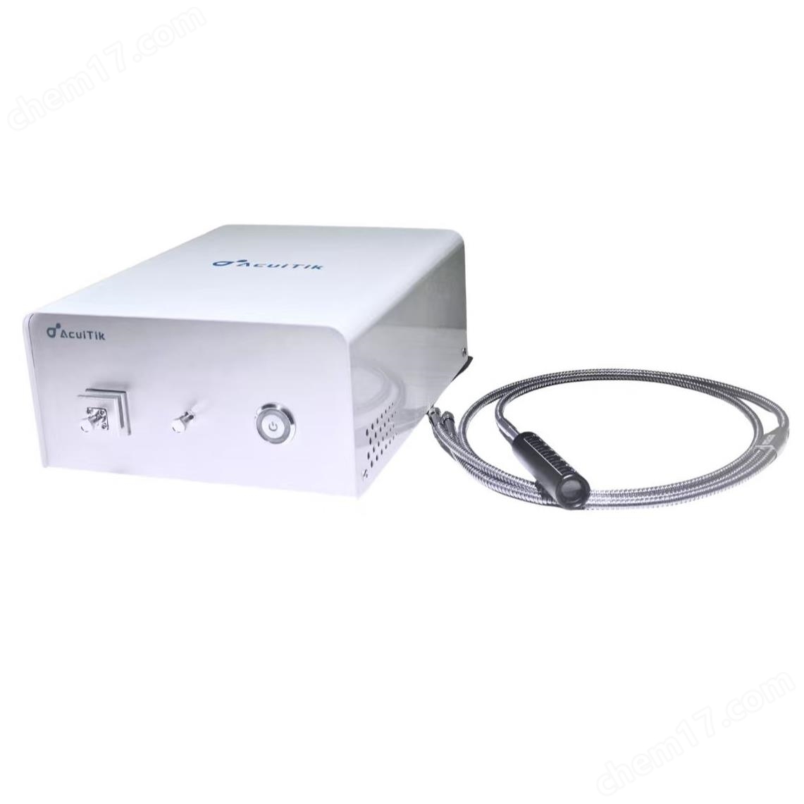
The NS-OEM series (film thickness measurement kit) is developed based on the NS-20 thin film thickness gauge. Its optical probe is designed to be compact and suitable for various installation environments. To ensure accurate measurement, the optical probe needs to be kept perpendicular to the surface of the sample. It is recommended to use our equipped angle adjustment tool to precisely adjust the installation angle. The optical probe is connected to the host via optical fiber, and the length of the fiber is flexible and variable, which can meet the installation requirements of different layouts.
Product Details
The NS-OEM series (film thickness measurement kit) is developed based on the NS-20 thin film thickness gauge and is used forMeasurement of thickness of solar perovskite multilayer films,Its optical probe is designed to be compact and suitable for various installation environments. To ensure accurate measurement, the optical probe needs to be kept perpendicular to the surface of the sample. It is recommended to use our equipped angle adjustment tool to precisely adjust the installation angle. The optical probe is connected to the host via optical fiber, and the length of the fiber is flexible and variable, which can meet the installation requirements of different layouts.
-Wavelength range: 190-1000 nm or 350-1100 nm
-Optical probes are designed for integration into automation equipment, online systems, vacuum chambers, in-situ growth chambers, and other special environments to meet diverse application needs.

Parameter Specifications

1. Depends on the tested sample material and the selected wavelength range;
2. Select standard thickness samples of silicon dioxide on silicon wafers (thickness range 500~1000nm);
3. Calculate the 1-fold standard deviation of 100 measurements of 500nm SiO2 standard plate, and take the average of the 1-fold standard deviation of 20 effective measurement days;
4. Depending on the complexity of the formula, the standard case is the formula for measuring the standard thickness of silicon dioxide on a silicon wafer.
Similar Product Recommend


