-
E-mail
info@phenom-china.com
-
Phone
18516656178
-
Address
Room T5705, Shanghai Hongqiao Libao Plaza, No. 88 Shenbin Road, Hongqiao Town, Minhang District, Shanghai
Product Categories
Funa Scientific Instruments (Shanghai) Co., Ltd

AFM-SEM synchronous combination technology (universal version)
NegotiableUpdate on 12/28
- Model
- Nature of the Manufacturer
- Producers
- Product Category
- Place of Origin
Overview
AFM-SEM synchronous combination technology (universal version) SEM and AFM are two widely used and complementary technologies in sub nanometer sample analysis. Integrating AFM into SEM can integrate the advantages of both, achieve an ultra efficient workflow, and accomplish extreme performance and complex sample analysis that is difficult or impossible to achieve with traditional AFM and SEM.
Product Details
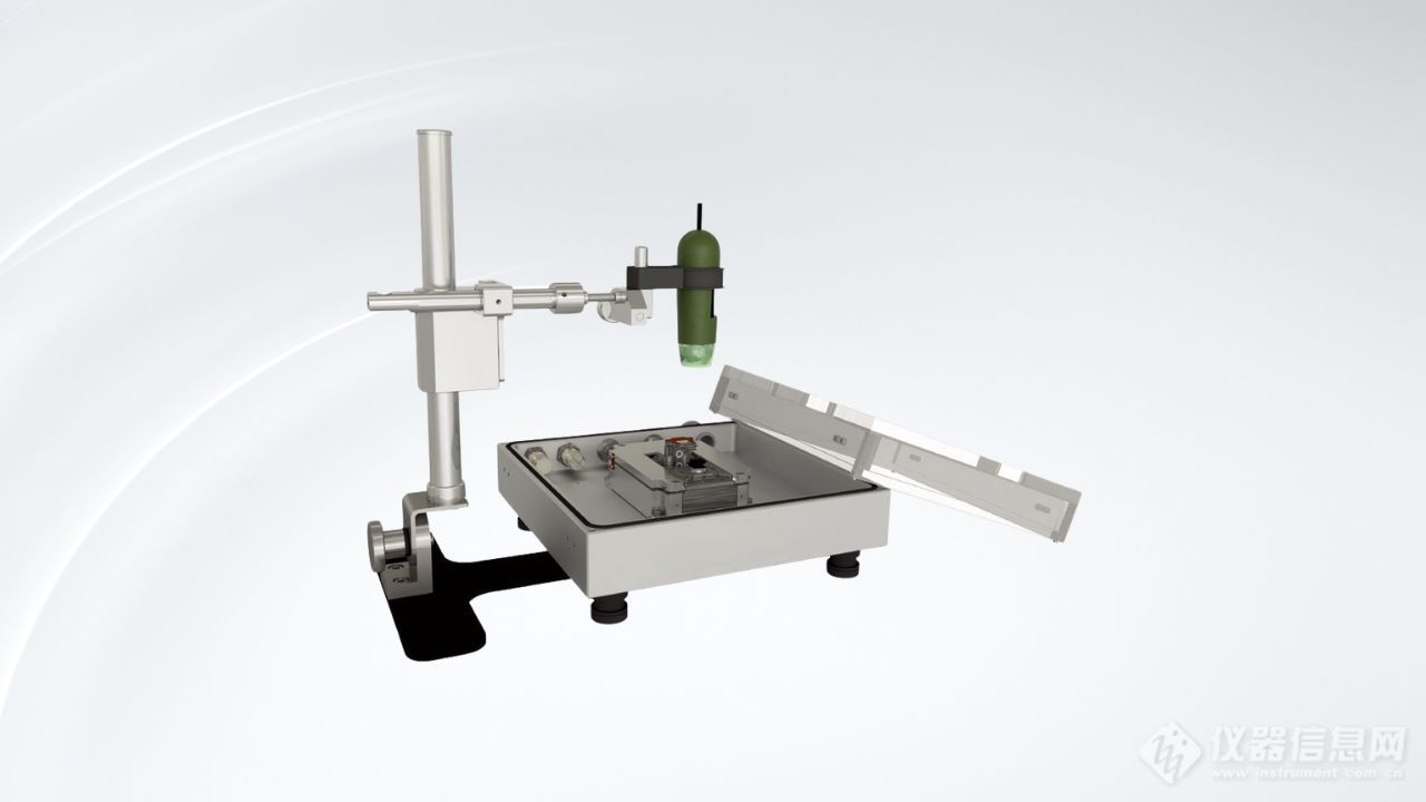
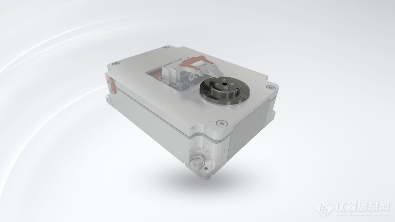
AFM-SEM synchronous combination technology (universal version)
Product Introduction
The revolutionary atomic force microscope (AFM) enables seamless integration with scanning electron microscopy (SEM), opening up new possibilities for in-situ correlation microscopy.
Thanks to optimized design, LiteScope AFM is compatible with Thermo Fisher Scientific TESCAN、 Mainstream brands such as Zeiss, Hitachi, JEOL, etc. have SEM systems and their accessories, and other brands of electron microscopes can also be customized and adapted.
Measurement mode:
• Mechanical properties: AFM, energy dissipation, phase imaging
• 电性能: C-AFM、KPFM、EFM、STM
• Magnetic properties: MFM
• Electromechanical: PFM
• Spectroscopy: F-z
Curve, I-V curve
• Correlation analysis: CPEM
AFM-SEM synchronous combination technology (universal version)
Practical features
In situ sample characterization
Ensure that sample analysis is carried out simultaneously, in the same location, and under the same conditions within the in-situ conditions of SEM, and atomic level resolution can also be achieved within the Feina electron microscope
-
Accurately locate the area of interest
The in-situ combination of SEM and AFM ensures analysis under the same time, location, and conditionsUsing SEM images to observe the relative position between the probe and the sample in real-time, providing navigation and precise positioning for the probe
-
Implement complex sample analysis requirements
Provides multiple measurement modes such as electrical, magnetic, and spectroscopic, and can be directly combined with SEM and EDS functions at the same location. Simultaneously obtain AFM and SEM data and seamlessly correlate them
Application Cases
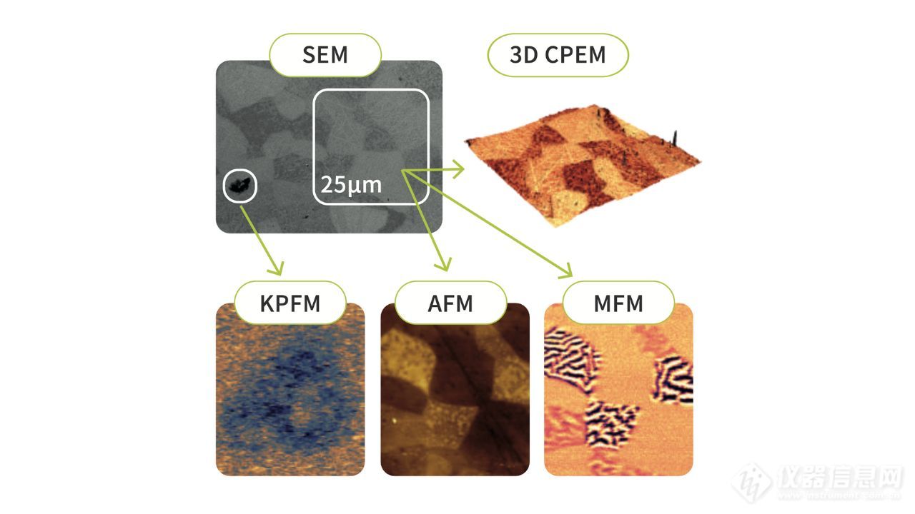
Composite analysis of steel and alloy
Composite analysis of dual phase steel using atomic force microscopy revealed surface morphology (AFM) and iron contentMagnetic domain structure (MFM), grain to grain ratio (SEM), and surface potential impurity Kelvin of ferrite grainsProbe force microscopy analysis method.• Related multimodal analysis reveals complex properties• Accurate positioning of ROI using scanning electron microscopy and comprehensive analysis using AFM
In situ characterization of batteries
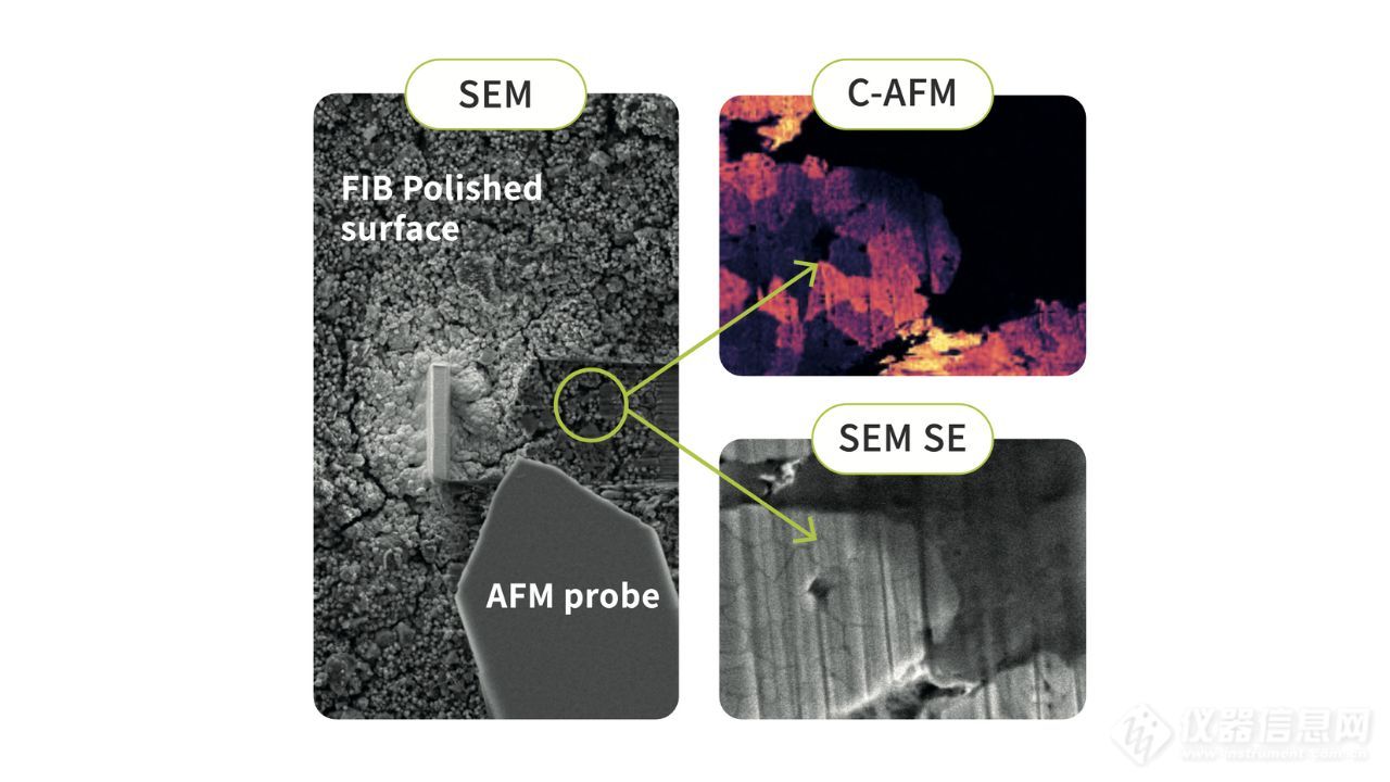
Solid state batteries (SSBs) exhibit higher energy density, longer lifespan, and more than lithium-ion batteriesGood security. Positive electrode tape composed of lithium nickel manganese cobalt oxide (NMC) particles in a glove boxAfter 200 cycles, it was opened, cut in situ, and measured using AFM in SEM.
Sample provided by Aleksandr Kondrakov, BELLA (DEU)
•Characterization of Local Conductivity (C-AFM) at CAM Cross Section
•In situ preparation of sensitive CAM without air exposure
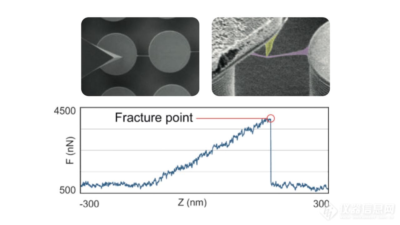
Excellent characterization of nanowires
Suspended spider silk nanowires have been studied for their mechanical properties using ultra precise positioning AFMSharp on suspended nanowires. Force distance spectroscopy enables determination of the elasticity and plasticity of nanowiresTransformation becomes possible.
Sample provided by Linnea Gustafsson, KTH (SWE).
• SEM: Real time observation of precise positioning of AFM tip and nanowire deformation
• Analyze properties such as Young's modulus and tensile strength
Optional accessories
Nanoindentation module
The nanoindentation module can simultaneously observe the sample using ultra-high magnification scanning electron microscopyConduct micro mechanical experiments and use LiteScope to perform sub nanometer resolution on indentation samplesanalyze
NenoCase and Digital Camera
Use LiteScope as an independent AFM under environmental conditions or different atmospheres, through digital meansCamera precise navigation probe.
Sample rotation module
Suitable for AFM analysis after FIB. In addition, it is allowed to install multiple samples simultaneously withoutMultiple samples can be tested by opening the SEM chamber.
Similar Product Recommend