-
E-mail
info@phenom-china.com
-
Phone
18516656178
-
Address
Room T5705, Shanghai Hongqiao Libao Plaza, No. 88 Shenbin Road, Hongqiao Town, Minhang District, Shanghai
Product Categories
Funa Scientific Instruments (Shanghai) Co., Ltd
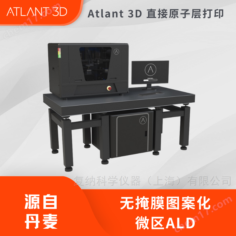
AAtlanta 3D Direct Atomic Layer Printing System
NegotiableUpdate on 12/28
- Model
- Nature of the Manufacturer
- Producers
- Product Category
- Place of Origin
Overview
ATLANT 3D has launched a direct atomic layer processing technology - a platform that can achieve atomic level precision, direct writing without masks, and in-situ processing of multiple materials. The aAtlanta 3D direct atomic layer printing system can achieve selective deposition, etching, doping, and surface modification, and achieve high-precision real-time control through software. Unlike the traditional ALD process of "full surface deposition+photolithography+etching", DALP allows materials to be deposited only at the required locations, truly achieving "on-demand manufacturing".
Product Details
AAtlanta 3D Direct Atomic Layer Printing System
「Atomic level manufacturing ushers in a paradigm shift''
With the rapid development of electronic, photon, quantum technology and aerospace manufacturing, the manufacturing industry is facing severe challenges: higher material precision, more complex device structures, higher performance and lower energy consumption, while also requiring stronger material and design flexibility. However, traditional material deposition techniques are gradually reaching their limits in terms of speed, vacuum requirements, photolithography steps, and material switching.


The traditional patterning process relies on masks and etching techniques
In order to break through the bottleneck, ATLANT 3D has launched Direct Atomic Layer Processing (DALP) ®) Technology - a platform that can achieve atomic level precision, direct writing without masks, and in-situ processing of multiple materials.
AAtlanta 3D Direct Atomic Layer Printing System
01. What is DALP ®?A groundbreaking atomic level direct writing technology
DALP ® It is an atomic level machining platform based on a micro nozzle system, which can achieve selective deposition, etching, doping, and surface modification, and achieve high-precision real-time control through software. Unlike the traditional ALD process of "full surface deposition+photolithography+etching", DALP ® Allow materials to deposit only in the required locations, truly achieving 'on-demand manufacturing'.


The working principle of DALP is based on spatial atomic layer deposition technology, which separates chemical precursors and reactants at the spatial level and independently transports them to specific locations on the substrate using a micro nozzle system. This ensures that chemical reactions only occur within the target area, thereby reducing cross contamination and improving accuracy. This process can achieve micrometer level lateral resolution and nanometer level thickness accuracy control.


DALP technology is based on the combination of spatial atomic layer deposition and 3D printing technology
When the nozzle moves on the substrate, material growth or etching occurs simultaneously, and real-time patterning can be achieved without traditional masking or post lithography steps. This method has many advantages, including local processing, strong scalability, suitability for industrial applications, and compatibility with various materials such as metals, oxides, and semiconductors.
「DALP ® The core characteristics of''
01 Maskless direct writing
Traditional ALD requires patterning through photolithography, while DALP ® Directly growing materials in the selected area can achieve:
Atomic level patterning with zero mask
Real time design modification
Eliminate material waste caused by photolithography and etching
It provides flexibility for rapid prototyping and agile manufacturing
02. Single step multi material integration
DALP ® Capable of continuously depositing multiple ALD processes in one process, covering the conventional ALD process library:
metal
oxide
nitride
sulfide
03. Software and AI driven adaptive manufacturing
Through machine learning algorithms, DALP ® can:
Real time monitoring of sedimentation status
Automatically optimize growth parameters
Improve repeatability and reduce errors
4. Integrated platform supporting deposition, etching, doping, and surface modification
It can be achieved in a single system:
Localized Etching (ALE)
Selective doping
Surface functionalization (multi-component)
05. Scalable, low energy consumption, environmentally friendly
DALP ® Operating at atmospheric pressure without the need for a large vacuum chamber, significantly reducing:
energy consumption
maintenance cost
Chemical consumption
Waste discharge
02. DALP ® Main application areas
DALP ® Its high precision, multi material, and software driven characteristics make it a core driving force for multiple cutting-edge industries.


01 Next Generation Semiconductor Manufacturing
As Moore's Law approaches its physical limit, device structures become increasingly complex, and traditional methods are unable to meet the requirements. DALP ® Being able to directly write atomic level materials without the need for photolithography is an ideal technology for the following applications:
Rapid development of GAA-FET, FinFET, and 3D IC
Accurate processing of interconnects and high dielectric materials
Construction of atomic level passivation layer
Exploration of New Neuromorphic Chip Materials
Its advantages include higher yield, lower material waste, and faster iteration speed.
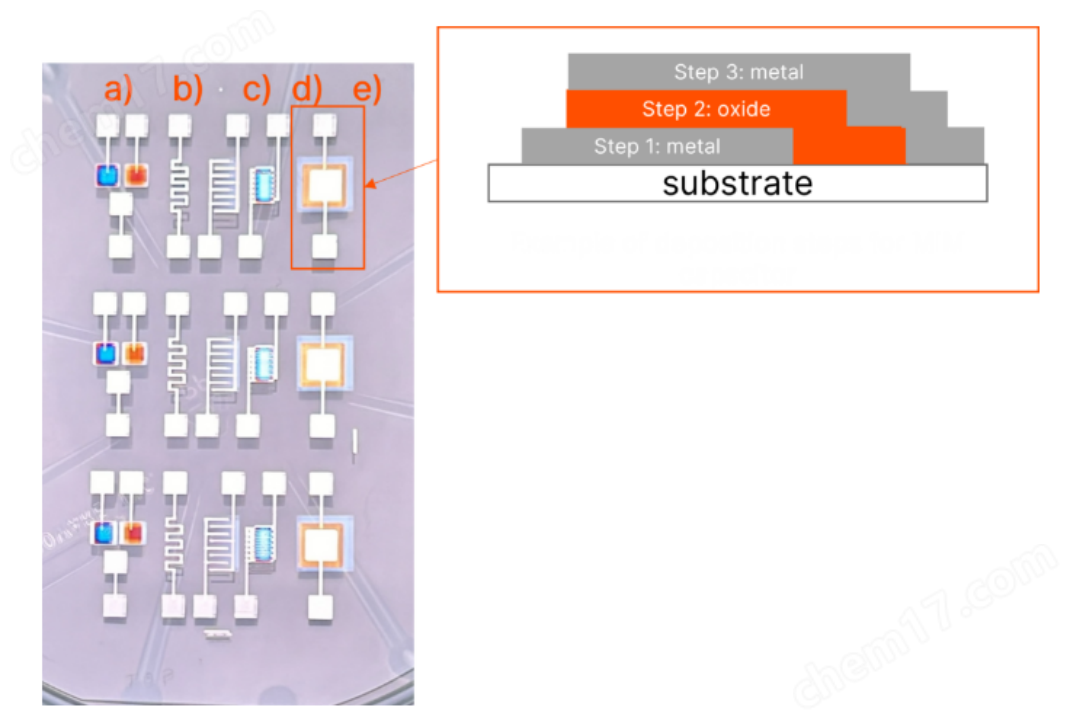

The diagram shows the use of DALP technology for gradient pattern deposition of metals and oxides in multi material devices
02. Photonics and Quantum Devices
Quantum computing and photonics require high material quality, requiring control of superconducting materials, optical coatings, and quantum materials at the atomic scale. DALP ® Can be directly written into:
optical waveguide
Superconducting quantum bit materials
Adjustable refractive index optical structure
Functional layers in photonic integrated circuits
No need for multiple chambers or steps, thereby reducing complexity and significantly speeding up the development cycle.


Using DALP to directly print coatings of different thicknesses in a single batch for waveguide testing
03. MEMS、 Sensors and Micro Electro Mechanical Systems
MEMS manufacturing typically involves multiple photolithography and deep reactive etching processes. DALP ® Provides a more direct and flexible approach:
Direct patterning of MEMS components (accelerometers, gyroscopes, resonators)
Deposition of functional layers on microfluidic chips
Biocompatible coatings for wearable and implantable sensors
This makes MEMS easier to customize, faster, and more economical

Deposition of gradient thickness TiO on Pt electrode using DALP2Coating for gas sensor research
04. Nanoscale accuracy, excellent uniformity, and adaptability to complex structures
DALP ® Its reliability and high performance have been verified in multiple experiments:
Accuracy and Alignment


Alignment accuracy target:~1 μ m
Alignment marks can be directly deposited on the sample
2. Thickness control

The thickness is linearly related to the number of cycles
Deviation of 8% at 10 nm
Deviation reduced to 1% at 270 nm
Repeated deviation after 3 months: 4%
3. High uniformity: The uniformity of the central area of multi material deposition is better than 1%


4. Conformal coatings on complex surfaces
DALP ® Can deposit on the following complex structures:

Anodized alumina (AAO) macropores with a roughness of 25 μ m
Nanostructured black silicon
High aspect ratio groove with a depth of 60 μ m
90 ° straight wall structure

Cross sectional view of platinum deposition in a 20 µ m channel capacitive sensor. The EDX elemental scanning results indicate that platinum is deposited in a conformal manner along the sidewall
05. DALP ® Defining future manufacturing
Direct Atomic Layer Processing (DALP) ®) Not only is it an advancement in material deposition technology, but it is also a cross era infrastructure for manufacturing. It compresses traditional dozens of steps into software controllable processes through maskless direct writing, multi material integration, AI driven manufacturing, and atmospheric pressure operation.
From lithography driven to software driven
From vacuum manufacturing to atmospheric pressure manufacturing
From multi cavity to integrated platform
Moving from fixed processes to adaptive intelligent manufacturing
With the increasing demand for high precision and material diversity in the industry, DALP ® It is becoming an important technological foundation for semiconductors, photonics, quantum computing, MEMS, and aerospace manufacturing. It is not a gradual improvement, but a revolution in atomic level manufacturing.
06. Regarding Atlant 3D and DALP technology
ATLANT 3D is a deep technology company founded in 2018 and headquartered in Copenhagen, Denmark, focusing on achieving "atomic level" manufacturing. Its core technology is DALP ® (Direct Atomic Layer Processing), Accurate material deposition and patterning can be achieved at the atomic level without the need for traditional masks or multi-step processes. The application areas served by the company include microelectronics, photonics, sensors, quantum computing, and space manufacturing. The development of DALP technology is the result of collaboration between multiple academic and industrial institutions.
Dr. Maksym Plakhotnyuk (Technical University of Denmark), Ivan Kundrata (Slovak Academy of Sciences), and Dr. Julien Bachmann (University of Erlangen Nuremberg): Their joint research on local deposition techniques was ultimately published in the book "Additive Manufacturing under Atomic Layer Processing Mode".
University of Grenoble and University of Lyon: Dr. David Mu ñ oz Rojas (Grenoble) is dedicated to improving space atomic layer deposition (ALD) technology, while Dr. Catherine Marichy (Lyon) is dedicated to research on direct surface structuring and maskless deposition methods. Their efforts have promoted the scalability and accuracy improvement of local ALD processes
Model recommendation-Nanofabricator Lite


NANOFABRICATOR ™ LITE enables rapid material and process testing, gradient based deposition, as well as experimental design and rapid development of device prototypes, shortening the research and development cycle from months to weeks. The integrated software equipped with it has a streamlined workflow, user-friendly interface, and supports industry standard file formats (GDS-II and DXF), enabling users to complete real-time structural design, preview, and adjustment, thereby accelerating innovation and application implementation.
For more product information and application details, please feel free to contact us
Similar Product Recommend