Founded in April 2015, NANO CHINA Co., LTD is a high-tech company serving customers in Greater China (including Chinese Mainland, Hong Kong, Taiwan, China and Macao), focusing on providing technical consultation, product sales and after-sales technical support for universities, research institutes, enterprise research and development and FAB factories.
Nano China's main products include thin film process systems, surface analysis and detection systems, wafer processing and measurement systems, as well as related systems involved in other micro - and nano scale processes.
In the field of thin film process systems, products cover thin film deposition equipment, thin film growth equipment, dry etching equipment, megasonic wet cleaning equipment, etc. Typical process systems involve PVD physical vapor deposition (magnetron sputtering, thermal vapor deposition, electron beam vapor deposition), CVD chemical vapor deposition (PECVD, ALD, PA-MOCVD, Parylene Perelin vacuum coating equipment), dry etching (RIE, ICP, DRIE, IBE, RIBE), wafer/mask cleaning systems (single crystal circle cleaning, megasonic cleaning), and application areas cover semiconductors MEMS、 Optoelectronics, nanotechnology, photovoltaics, etc.
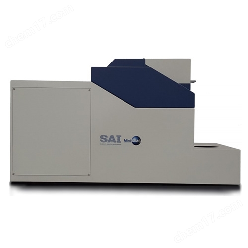
In the field of surface analysis and detection, the products involve Time of Flight Secondary Ion Mass Spectrometer (TOF-SIMS) and Matrix Assisted Laser Desorption Ionization Time of Flight Mass Spectrometer (MAIDI ToF MS) for material surface analysis applications.
In the field of wafer processing systems, the products are mainly precision wafer scribers used for scientific research and small-scale production. In the field of wafer measurement systems, the products mainly include wafer thickness TTV, surface flatness, bending Bow, bending Warp, thin film stress, resistivity resistance measuring instruments, as well as wafer contact angle measuring instruments (Wafer Contact Angle Measuring System) used for wafer contact angle measurement.
We have won widespread recognition and support in the market with our rich industrial technical experience, gradual marketing network and professional after-sales technical support. Hundreds of sets of equipment we have sold are distributed in universities, research and development centers and State Key Laboratory in more than 20 different countries.
We hire skilled and well-educated design and manufacturing engineers, application engineers, service engineers, and technical support personnel, enabling the company to have a top-notch service team. As a provider of thin film process equipment and surface analysis instruments, our goal is to provide high-quality services and always maintain the highest level of integration.