-
E-mail
sende_services@outlook.com
-
Phone
17688459448
-
Address
No. 983 Huangpu Avenue East, Huangpu District, Guangzhou City, Guangdong Province
Product Categories
Guangdong Sende Instrument Co., Ltd
scanning electron microscope
NegotiableUpdate on 02/08
- Model
- Nature of the Manufacturer
- Producers
- Product Category
- Place of Origin
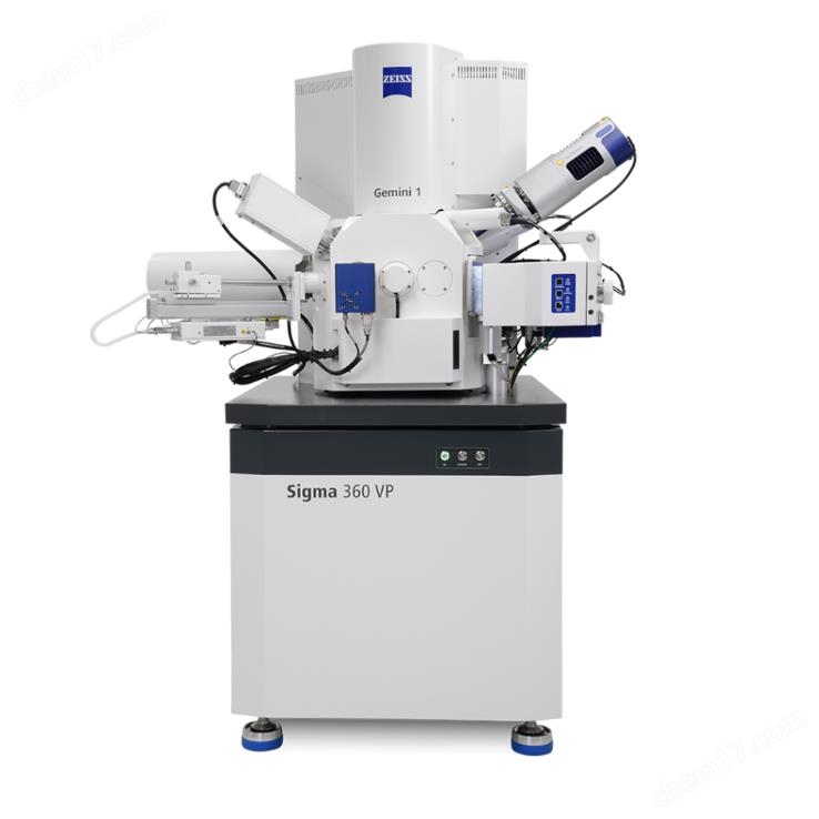
Overview
Zeiss Sigma series products feature field emission scanning electron microscopy (FE-SEM) with high-quality imaging and advanced microscopic analysis capabilities
Product Details
scanning electron microscope
Having high-quality imaging and advanced differential resolutionFE-SEM for functional analysis
Zeiss Sigma Series Product CollectionfieldEmission scanning electron microscopeThe integration of FE-SEM technology and excellent user experience enables easy implementation of imaging and analysis programs, improving work efficiency. You can use it for quality monitoring of new materials and particles, or for research on biological and geological samples. Striving for excellence in high-resolution imaging - using low voltage to achieve better resolution and contrast at 1 kV or lower voltage. Its excellent EDS geometry design enables advanced microscopic analysis, obtaining analysis data at twice the speed and with higher accuracy.
·Sigma 360It is an intuitive imaging and analysis toolFE-SEMIt is an ideal choice for analysis and testing platforms.
·Sigma 560 adopts EDS geometry design, which can provide high-throughput analysis and achieve automatic in-situ experiments.


The optical system of Gemini 1
The optical system of Gemini 1 consists of three components: an objective lens, an electron beam thruster, and a detector with Inlens detection principle. Among them, the design of the objective combines the forces of electrostatic and magnetic fields, greatly optimizing optical performance while reducing the influence of the field in which the sample is located. This can also achieve high-quality imaging of challenging samples such as magnetic materials. The Inlens detection principle ensures efficient signal detection by detecting secondary electrons (SE) and/or backscattered electrons (BSE), while significantly reducing the time required to acquire images. The electron beam thruster ensures small-sized electron beam spots and high signal-to-noise ratio.

Flexible detection
Sigma is equipped with a range of different detectors to characterize your samples through new detection techniques. The high vacuum mode using ETSE and Inlens detectors can obtain high-resolution information on surface morphology. Clear images can be obtained using the variable pressure mode of VPSE or C2D detectors. High resolution transmission electron imaging can be performed using aSTEM detectors. By using different optional BSE detectors (such as aBSD detectors), the composition and surface morphology of the sample can be studied in depth.

NanoVP lite mode
By using NanoVP lite mode for analysis and imaging, higher image quality can be obtained under low voltage conditions, and more accurate analysis data can be obtained more quickly.
·In NanoVP lite mode, the skirt effect decreases and the path length of the incident beam (BGPL) decreases. Reducing the skirt edge will improve the signal-to-noise ratio of SE and BSE imaging.
·The telescopic aBSD with five arcs provides excellent material composition contrast: During the operation of NanoVP lite, the detector is equipped with a beam sleeve installed below the pole shoe, which can provide high-throughput and low-voltage composition and surface morphology high contrast imaging, suitable for variable pressure and high vacuum conditions.
Life Sciences
Learn more about the microscopic and nanostructured information of protozoa or fungi, and obtain the ultrastructure on cross-sectional samples or thin sections.


Earth Science and Natural Resources
Explore rocks, ores, and metals.


industrial applications
Understand how to conduct research on metals, alloys, and powders.


![]()

Similar Product Recommend