-
E-mail
sende_services@outlook.com
-
Phone
17688459448
-
Address
No. 983 Huangpu Avenue East, Huangpu District, Guangzhou City, Guangdong Province
Product Categories
Guangdong Sende Instrument Co., Ltd

Field emission scanning electron microscope
NegotiableUpdate on 02/08
- Model
- Nature of the Manufacturer
- Producers
- Product Category
- Place of Origin
Overview
GeminiSEM460 can help you easily achieve sub nanometer resolution imaging. Excellent imaging and analysis techniques further enhance FE-SEM (Field Emission Scanning Electron Microscopy).
Product Details
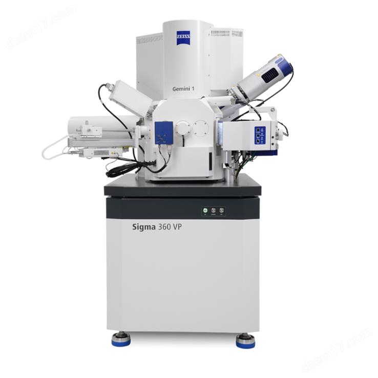
Zeiss GeminiSEM 460
FE-SEM meets the high requirements for sub nanometer imaging, analysis, and sample flexibility
Zeiss GeminiSEM can help you easily achieve sub nanometer resolution imaging. Excellent imaging and analysis techniques further enhance FE-SEM(Field emission scanning electron microscope)Like adding wings to a tiger. We adopt innovative electronic optical systems and a brand new sample chamber design, which not only makes operation easier and usage more flexible and diverse, but also brings you higher image quality. Sub nanometer level images below 1 kV can be captured without immersion of the objective lens in water. Explore three designs of Zeiss Gemini electro-optical system:
lThe ideal choice for analysis and testing platform - Zeiss GeminiSEM 360
lEfficient Analysis - Zeiss GeminiSEM 460
lNew standard for surface imaging - Zeiss GeminiSEM 560
GeminisEM 460Field emission scanning electron microscopeDesigned specifically for demanding analytical tasks, it enables efficient analysis and automated workflows. When facing challenging analytical tasks in the field of microscopy, its Gemini 2 tube can lend a helping hand, with seamless switching between imaging and analysis conditions.
✔Balancing high resolution and high current
✔Customize automated workflow
✔Bringing you more possibilities

Balancing high resolution and high current
✔ The GeminiSEM 460 is designed specifically for demanding analytical tasks, enabling efficient analysis and automated workflows.
✔ Quickly perform high-resolution imaging and analysis: Use Gemini 2 tube to seamlessly switch from low beam low voltage working conditions to high beam high voltage working conditions (or vice versa).
✔ Meanwhile, multiple detectors can be used to characterize any sample from multiple directions.
✔ Efficient analysis can be conducted using a multifunctional sample chamber, and suitable analysis detectors can also be selected.
✔ In the new VP mode, increase the current to achieve EBSD imaging with a count rate of 4000 points per second.
✔ By using two geometrically symmetrical EDS ports and a coplanar EDS/EBSD configuration, chemical composition and crystal orientation can be detected, achieving high-speed, shadowless EDS/EBSD imaging.

Customize automated workflow
✔ Due to such powerful analytical capabilities, automation of workflow becomes crucial. By using Zeiss' Python scripting API, you can create and configure your own automated experimental process.
✔ Modify the experimental process according to your personalized needs and tailor the desired effect.
✔ Fully utilize the imaging capabilities of STEM tomography: effectively combine automatic tilt and rotation functions with feature tracking functions, and after sending all aligned images to dedicated 3D reconstruction software, construct 3D tomography with nanometer level resolution.
✔ If you need to test the material's bearing limit, Zeiss will provide you with an experimental platform for performing automated in-situ heating and tensile experiments. During the experiment, the material's condition under heating and stretching can be automatically presented to you, and the stress-strain curve can be drawn in real time.

Bringing you more possibilities
✔ Based on the design of Gemini 2 tube, the analytical capability under ultra-high and adjustable current density conditions is significantly improved when used in the fields of materials and life sciences, even under low voltage conditions.
✔ You can make full use of various accessories to upgrade the system. For example, not only can analytical equipment be added, but also in-situ experimental equipment, cryogenic imaging, and nanoprobes can be used to configure multifunctional sample chambers. Storage allows you to connect data collected from different devices in the laboratory, enabling centralized project management.
✔ During the use of the device, various configurations can be easily assembled and upgraded at any time.
✔ All GeminiSEMs have joined the Zeiss ZEN core ecosystem, which allows you to access ZEN Connect, ZEN Intellesis, and ZEN's analysis module, helping you generate reports and implement GxP workflows.
Fully utilize rapid analysis
The comprehensive characterization of any sample requires high-performance imaging and analysis, and today's users expect devices to be easy to set up and operateGemini 2 OpticsThe system can meet these requirements.

High resolution imaging and analysis can be seamlessly switched
The GeminiSEM 460 is equipped with a Gemini 2 optical system with dual focusing lenses.
Continuously adjust the current intensity of the electron beam while optimizing the beam spot size.
Seamless switching between high-resolution imaging with low beam and analysis mode with high beam.
No calibration is required after changing imaging parameters, saving time and effort.

Maintain flexibility and work efficiently
✔ Maintain flexibility: Use high electron beam energy density for high-resolution imaging and analysis at low and high beam currents, unaffected by the electron beam energy you choose.
✔ The sample will not be exposed to a magnetic field: achieving distortion free EBSD patterns and high-resolution imaging within a large observation field.
✔ When the sample is tilted and rotated, it does not affect the performance of the electron optical system, and magnetic samples can also be easily imaged.
✔ Choose the appropriate charging mode for the sample: local charge compensation, variable pressure inside the chamber, or NanoVP.


3D STEM tomography imaging
Now, you can freely perform automatic STEM tomography imaging on FE-SEM. A script using an API for automatically capturing STEM tilt series can perform center rotation, stage tilt movement, as well as automatic focusing and image acquisition. In addition, feature tracking can compensate for the offset of the entire tilted series and keep the drift between two images at a minimum of about 50 nm. STEM sample carriers allow the stage to tilt 60 ° and rotate 180 °, and aSTEM detectors can cover all requirements. Finally, the 3D reconstruction software from the Advanced Refactoring Toolkit (ART) development team utilizes this output to render the 3D model of your sample.
Similar Product Recommend