-
E-mail
sende_services@outlook.com
-
Phone
17688459448
-
Address
No. 983 Huangpu Avenue East, Huangpu District, Guangzhou City, Guangdong Province
Product Categories
Guangdong Sende Instrument Co., Ltd

Field emission scanning electron microscope
NegotiableUpdate on 02/08
- Model
- Nature of the Manufacturer
- Producers
- Product Category
- Place of Origin
Overview
Zeiss GeminiSEM can help you easily achieve sub nanometer resolution imaging. Excellent imaging and analysis techniques further enhance FE-SEM (Field Emission Scanning Electron Microscopy).
Product Details
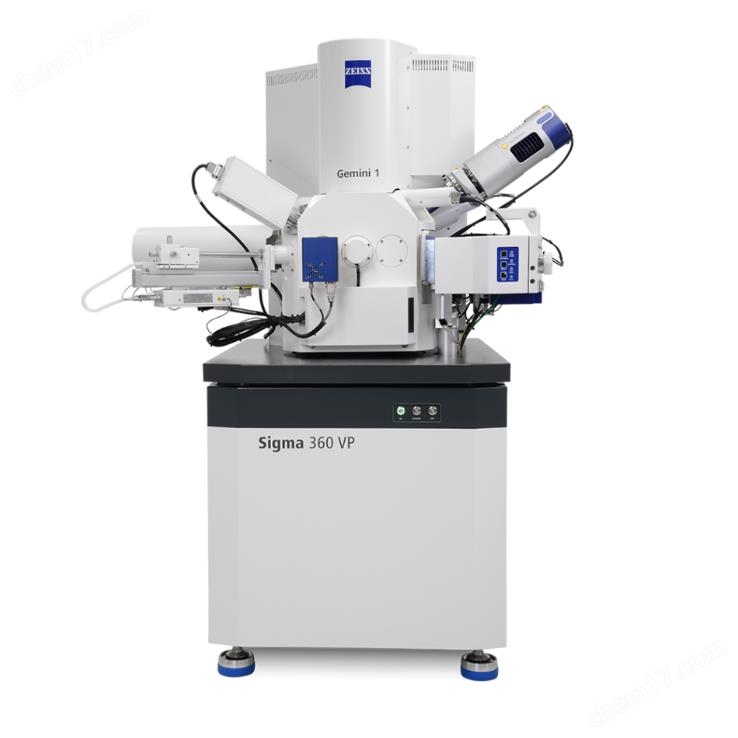
Zeiss GeminiSEM 560
FE-SEM meets the high requirements for sub nanometer imaging, analysis, and sample flexibility
Zeiss GeminiSEM can help you easily achieve sub nanometer resolution imaging. Excellent imaging and analysis techniques further enhance FE-SEM(Field emission scanning electron microscope)Like adding wings to a tiger. We adopt innovative electronic optical systems and a brand new sample chamber design, which not only makes operation easier and usage more flexible and diverse, but also brings you higher image quality. Sub nanometer level images below 1 kV can be captured without immersion of the objective lens in water. Explore three designs of Zeiss Gemini electro-optical system:
lThe ideal choice for analysis and testing platform - Zeiss GeminiSEM 360
lEfficient Analysis - Zeiss GeminiSEM 460
lNew standard for surface imaging - Zeiss GeminiSEM 560

GeminiSEM 560Field emission scanning electron microscopeThe standard for surface sensitivity, distortion free, and high-resolution imaging has been comprehensively improved, enabling easy imaging under conditions below 1kV. It also introduces Gemini 3 tube and a new electronic optical engine SmartAutopilot, which can achieve high resolution of the series under any working conditions.
✔New standards for surface imaging
✔Integrate professional knowledge
✔Experience excellent contrast


Easily achieve imaging below 1kV
✔ The Gemini 3 tube is used for leak free magnetic imaging at voltages below 1 kV and resolutions below 1 nm, without the need for sample stage bias or monochromator. It includes Nano win objective lens and a brand new electronic optical engine Smart Autopilot.
✔ By adopting a new variable pressure mode and detection system, images of non-conductive substances can be obtained: in VP mode, after passing through a low light toxicity sample exchange chamber, vacuum sensitive samples are placed in the sample chamber to ensure fast results while retaining features.
✔ Utilizing dual EDS portsThe brand new large sample warehouse makes it easy to analyze fine samples. Excellent detector solid angle ensures fast, shadow free imaging for you.

Integrate professional knowledge
✔ The observation field of the system is greatly increased, making it easy to perform simple sample navigation.
✔ For samples with extremely strict requirements, the new electronic optical engine Smart Autopilot significantly improves imaging speed. It can save time and eliminate the need for time-consuming focusing: this engine can drive an electronic optical system with a magnification range from less than 1 to up to 500000 times, and can automatically center, calibrate, and focus throughout the entire process. Getting a brand new parallax autofocus is also included, and the new automatic swing function provides you with clear images within seconds.
✔ Python scripts can use these functions in automated workflows such as 3D STEM tomography imagingcan

Experience excellent contrast
✔ Finding effective points within the working conditions you have set means that you have selected the correct parameter combination, and the key to achieving an ideal image is to find that parameter combination. Gemini's leak free magnetic technology and its new Gemini 3 tube can present you with the ideal parameter combination to help you explore new information.
✔ The magnetic field on the sample is less than 2 mT, making it easy to achieve magnetic domain contrast imaging. Energy spectral imaging can be performed using Inlens backscatter detectors with selectable energy, while electronic annular spectral imaging can be performed using annular backscatter detectors.
✔ Collect all data together using ZEN Connect, detailedShare and report your findings.
Imaging below 1kV - Integrating Professional Knowledge
The Gemini 3 optical system optimizes resolution at low and extremely low voltages and achieves contrast enhancement, ensuring high-resolution imaging under all operating conditions from 1 kV to 30 kV. It includes two components that work together: a Nano win objective lens and a new electronic optical engine, Smart Autopilot. In addition, it also features a high-resolution electron gun mode and optional sample stage deceleration technology (Tandem Decel).
Resolution mode - allows you to see more details
More details and detection signals of SEM images can be obtained through two modes. In high-resolution electron gun mode, the color difference of the electron beam is reduced, thereby achieving smaller beam spots; In the deceleration technology mode of the sample stage, applying a deceleration voltage to the sample can further improve the image resolution below 1 kV and enhance the detection efficiency of the backscatter detector.

Advantages of Nano win Objective:
● Achieve sub nanometer resolution at low and ultra-low voltages, achieving better signal detection efficiency.
Compared with the standard Gemini objective, the object image difference at low voltage is reduced by three times, resulting in a three fold decrease in the magnetic field on the sample, approximately 1 mT.
Optimize the geometric structure and the distribution of electrostatic and magnetic fields.
The signal of the Inlens detector is enhanced under low voltage imaging conditions.
These features provide the ability to achieve sub nanometer level imaging under conditions below 1 kV without the need to immerse the sample in an electromagnetic field.

Working Principle:
Smart Autopilot optimizes the electronic trajectory through the lens barrel, ensuring the highest possible resolution at each acceleration voltage.
This automatic function enables seamless alignment and free switching across the entire magnification range (from 1x to 2000000x), and increases the viewing field by 10x, allowing for imaging of objects up to 13cm in a single image.
32k × 24k image storage resolution combined with a new overview modeEnsure seamless pixel density within a large observation field.
Industrial microscope solution
Typical tasks and applications
●Failure analysis of mechanical, optical, or electronic components
●Fracture analysis and metallographic research
●Surface, microstructure, and device characterization
●Composition and phase distribution
●Identify impurities and inclusions

Applications in Life Sciences
Typical tasks and applications
●Characterization of topological structure
●Imaging of sensitive, non-conductive, degassed, or low contrast samples
●High resolution imaging of ultrastructure of cells, tissues, etc
●Perform large-area imaging, such as continuous slice or sectional imaging


Similar Product Recommend