-
E-mail
sende_services@outlook.com
-
Phone
17688459448
-
Address
No. 983 Huangpu Avenue East, Huangpu District, Guangzhou City, Guangdong Province
Product Categories
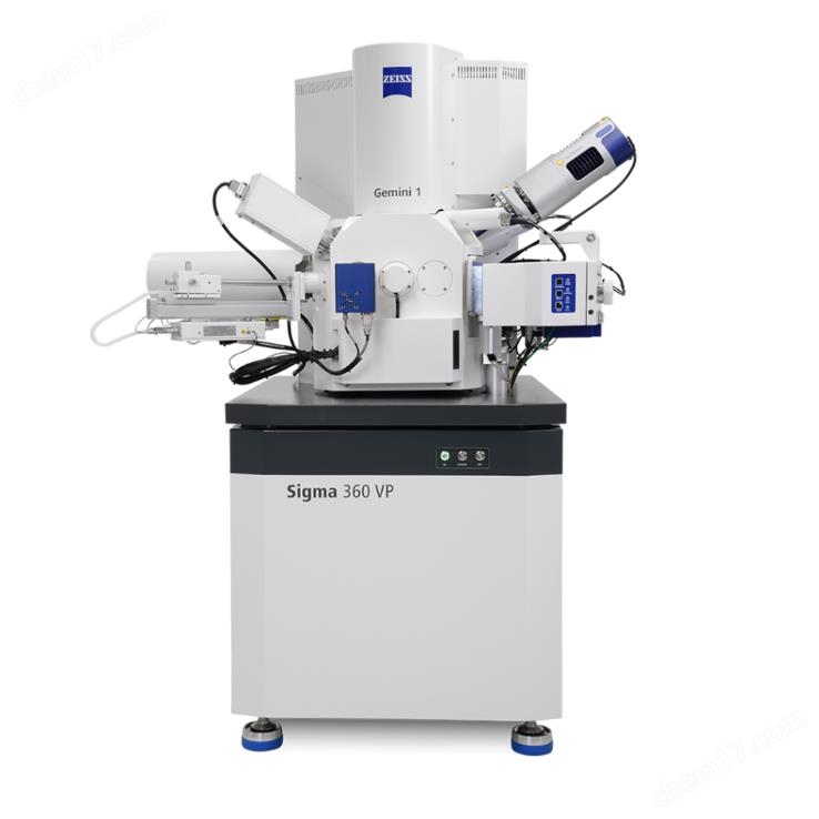
Guangdong Sende Instrument Co., Ltd

scanning electron microscope
NegotiableUpdate on 02/07
- Model
- Nature of the Manufacturer
- Producers
- Product Category
- Place of Origin
Overview
The Zeiss EVO series is a modular scanning platform with intuitive operation, suitable for daily inspection and research applications. The EVO series combined with high-performance scanning electron microscopes brings an intuitive and easy to operate user experience for microscope experts and new users.
Product Details
Zeiss EVO series
Intuitive modular operationscanning electron microscopePlatform, suitable for daily testing and research applications
EVO series combined with high performancescanning electron microscopeTo provide an intuitive and easy-to-use user experience for microscope experts and new users. With a wide range of options, EVO can be customized according to your needs, whether in life sciences, materials science, or daily industrial quality assurance and failure analysis.
lMulti functional solutions for microscope centers or industrial quality assurance laboratories
lObtain excellent images of real samples
lHigh image quality achieved using lanthanum hexaboride (LaB6) emitter
lConduct tests on non-conductive and uncoated samplesExcellent imaging and analysis
lWorkflow automation and data integrity


Intelligent navigation and imaging
Improve your sample processing throughput, enhance work efficiency and performance

Zeiss Navigation Camera
The camera can be installed in the sample chamber to monitor the relative position between the sample and the backscattered detector pole shoe(Sample warehouse camera);Or installed on the door of the vacuum sample chamber(navigation camera)Provide an overview of the arrangement of samples or components on the sample carrier. This view can be used to preset the regions of interest identified by optical microscope images and enable easy navigation throughout the entire sample detection process.

Automated intelligent imaging
EVO can automatically complete automated image acquisition of cross batch samples without human supervision. Zeiss automated intelligent imaging is very suitable for daily detection applications. Users can define boundary areas, automatically generate regions of interest determined by the desired observation field or magnification, and start automatic image acquisition, thereby improving your sample processing throughput, work efficiency, and performance.
Entering a new era of detection applications
Obtaining richer data using LaB6 electron gun
Compared to traditional needle type tungsten filaments, the electron emission of lanthanum hexaboride cathodes can be customized to ensure that every detail of the image is displayed according to your needs. You will benefit from the following two aspects:
lWith the same size (such as resolution) of the electron probe, you can achieve higher probe current, making image navigation and optimization easier.
lIn the case where the probe beam current (signal-to-noise ratio) remains constant, the beam diameter is much smaller, which can improve image resolution.
EVO can be well interconnected with other microscopes
Benefit from workflow automation and associated microscopy technology


application
Manufacturing and assembly industry
lquality analysis/quality control
lFailure Analysis/金相研究
lCleanliness inspection
ltalismanParticle morphology analysis in accordance with ISO 16232 and VDA 19 Part 1-2 standardsAnd chemical analysis
lAnalysis of non-metallic inclusions


Semiconductors and Electronicscomponent
lElectronic components, integrated electronicsRoads, MEMS devices, andVisual inspection of solar cells
lCopper wire surface and crystal structure detection
lMetal corrosion detection
lSection Failure Analysis
lWelding foot detection
lSurface imaging of capacitors


Steel and other metals
lImaging and analysis of the structure, chemical properties, and crystal structure of metal samples and inclusions
lPhase, particle size, welding, and failure analysis


raw materials
lMorphological, mineralogical, and compositional analysis of geological samples
lImaging and analysis of metal structures, fractures, and non-metallic inclusions
lAnalysis of morphology and composition of raw materials, chemicals, and active ingredients during micronization and granulation processes


Materials Science Research
lCharacterization of conductive and non-conductive material samples in research applications


Life Sciences
lResearch on plants, animals, and microorganisms


forensic medicine
lGunshot residueGoods (GSR)
lAnalysis of Coatings and Glass
lCoin forgery
lComparison of hair and fiber
lForensic toxicology


Similar Product Recommend