- Phone
-
Address
Building A, Future City, No. 147 Luoshi South Road, Hongshan District
Product Categories
Maikono Technology Co., Ltd
Line width measurement
NegotiableUpdate on 05/06
- Model
- Nature of the Manufacturer
- Producers
- Product Category
- Place of Origin
Overview
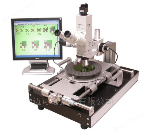
COMEF is an image processing software with special features designed for high-precision measurement of line width and spacing. Through the grayscale algorithm, it can measure the width and spacing of wires or structures on silicon wafers with sub-pixel accuracy.
Product Details
COMEF is an image processing software with special features designed for high-precision measurement of line width and spacing. Through the grayscale algorithm, it can measure the width and spacing of wires or structures on silicon wafers with sub-pixel accuracy.
It applies the principle of optical imaging reversibility. Therefore, people can also imagine placing the CCD chip in the object plane (sample plane). A microscope objective that images the test sample at the chip level at a magnification of 10x will, in principle, also image the chip at the test sample level at a magnification of 1/10.
What is sub-pixel processing? Subpixeling means, detection of edge position with higher reproductibility than ΔXm. Subpixel means detecting edge positions with higher reproducibility than Δ Xm. How does that work? How does this work? A condition is that the recognition of the edge position does not take place manually any longer via setting measuring points on the PC monitor. The condition is that the recognition of edge positions is no longer done by manually setting measurement points on a computer monitor. The edge recognition is made on the basis of grey tone distributions by the regarded screen window. Thus this measuring procedure no more is suitable for all kinds by objects. Edge recognition is based on the grayscale color distribution of the observed screen window. Therefore, this measurement method is no longer applicable to all types of objects. It works however outstanding perfect for all linear expanded objects, thus e.g. for circuit paths on hoppers or structures on wafers and masks in semiconductor technology. However, it performs well and is applicable to all linearly extended objects, such as circuit paths in semiconductor technology, structures on hoppers, and constructions on wafers and masks.
Due to the original pixel size of 6 microns on the chip, the size of each pixel at the test sample level is 0.6 microns.