- Phone
-
Address
Building A, Future City, No. 147 Luoshi South Road, Hongshan District
Product Categories
Maikono Technology Co., Ltd


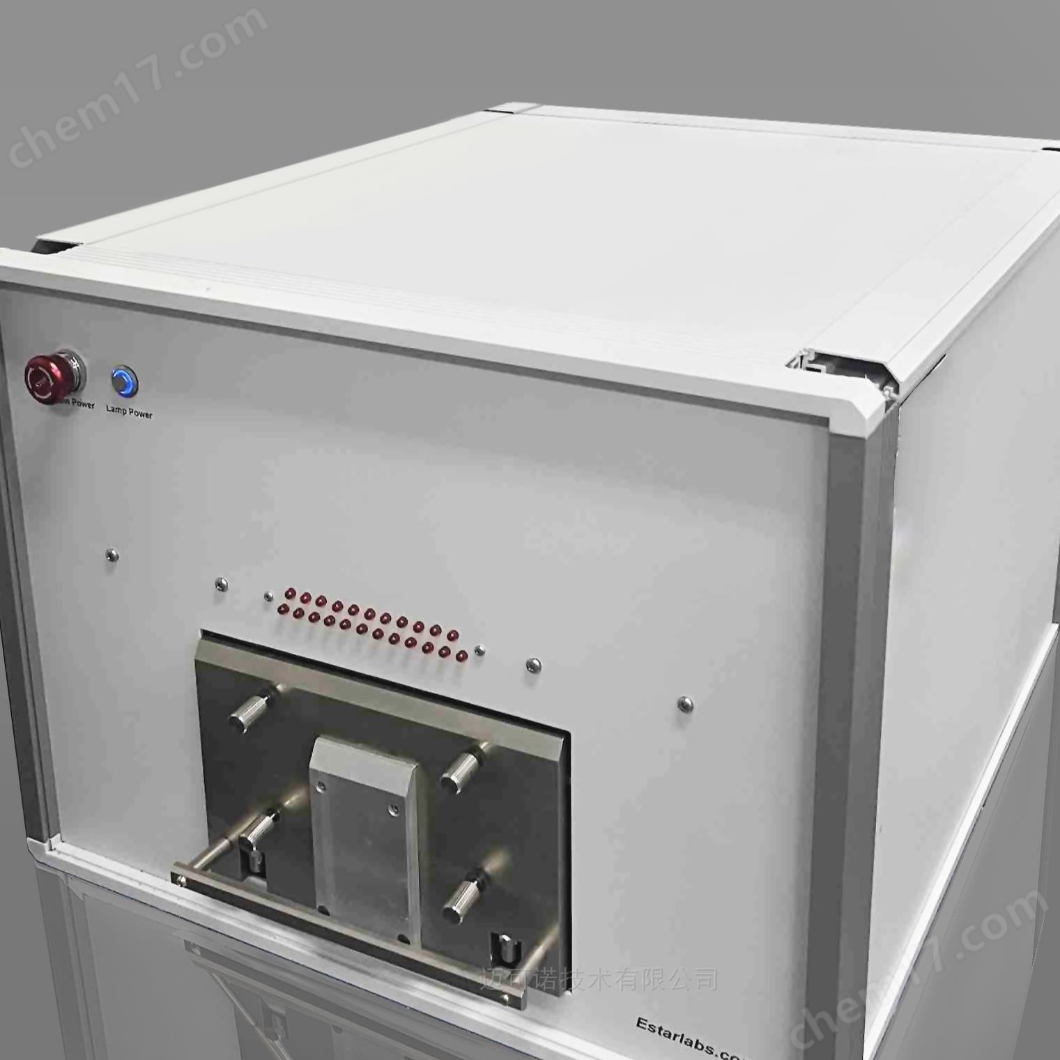
12 inch vacuum annealing furnace
NegotiableUpdate on 05/06
- Model
- Nature of the Manufacturer
- Producers
- Product Category
- Place of Origin
Overview
12 inch vacuum annealing furnace with multi zone temperature control, temperature uniformity can be adjusted through the APP interface. An excellent light source cooling system ensures that the lifespan of the light source meets international standards. The scientific wavelength distribution ensures that semiconductor materials can effectively absorb.
Product Details
12 inch vacuum annealing furnace
1.Temperature range:150–1,300℃;
2.Heating rate:1-200℃/Adjustable in seconds;
3.Temperature uniformity: ±5℃(200mm wafer 1015℃);
4.Sample size:12Inch or300×300mm(Multi temperature zone control);
5.Control software and hardware: self-developed system software, supportingSEMIAutomation standards,SECS/GEMCommunication interface; Programmable temperature curve storage500Above Article,Each curve includes50Above the paragraph, data can be exported as text files for easy data processing.
6.降温速率:80℃/Seconds (optional for rapid cooling, cooling rate)200℃/Seconds);
7.Temperature setting range:100-1,300℃, set range for each time period1- 30,000Seconds;
8.Temperature overshoot:<5℃;
9.Temperature measurement system:KType thermocouple, dual point temperature measurement (optical temperature measurement optional);
10.Cooling system:CDAWater cooling;
11.Temperature control accuracy: ±0.3℃;
12.PIDTemperature control:PIDTemperature control, ensuring no overshoot even at the heating rate;
13.Insulation time:1200℃ insulation time>600Seconds;
14.Temperature steady-state stability: ±1℃;
15.Process gas path:2roadMFC(Maximum optional)6Road);
12 inch vacuum annealing furnace application areas:
Silicon based, third-generation, and fourth generation semiconductor process technologies (RTP, RTA, RTO, RTN)
Research on Ferroelectric Materials
Thin film stress regulation
Integrated Circuit Manufacturing
Heat treatment before material property testing, thermal vibration test
CMOS process optimization
Doping activation (annealing after ion implantation)
Ohmic contact annealing (metalization annealing)
Oxidation/Nitriding Treatment
High k medium heat treatment
Surface treatment of silicon wafer
Manufacturing of solar cells
Phase change material processing
Thin film stress regulation
Grain growth and crystal annealing
Research on Thermal Stability of New Materials
MEMS device processing
Nanodevice processing