- Phone
-
Address
Building A, Future City, No. 147 Luoshi South Road, Hongshan District
Product Categories
Maikono Technology Co., Ltd

EBR measurement system
NegotiableUpdate on 05/06
- Model
- Nature of the Manufacturer
- Producers
- Product Category
- Place of Origin
Overview
When applying photoresist, anti reflective coating or polyimide coating on microelectronic substrates through spin coating, so-called edge protrusions are often formed. This is an unnecessary accumulation of coating material in the form of protrusions on the outer edge of the substrate. These accumulations may also wrap around the edges of the substrate, contaminating the edge area on the back of the substrate. If the wafer edge is not cleaned, dry particles or photoresist residues may peel off, leading to particle contamination and other issues in subsequent manufacturing and process steps. Therefore, excess residue in the peripheral area of the substrate should be removed. For this purpose, specialized equipment is available for use.
Product Details
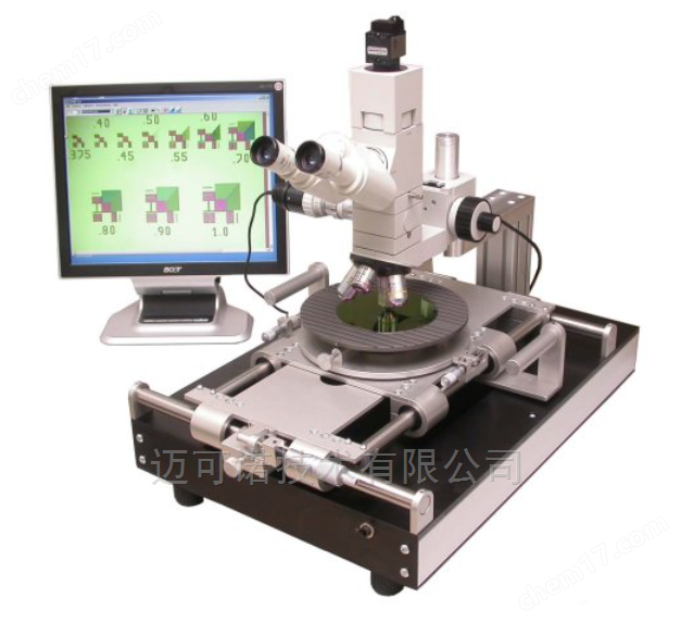
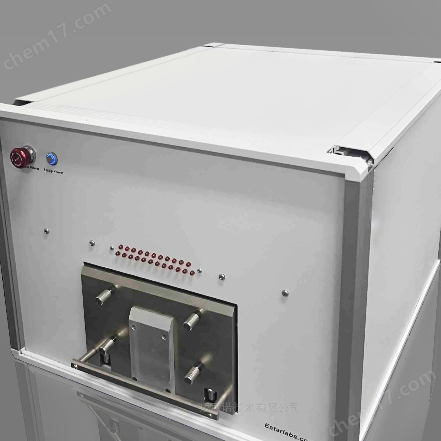
The EBR measuring device from OEG GmbH is used to check the function of the machines for Edge Bead Removal.
The EBR measuring device produced by OEG GmbH is used to detect the function of edge debonding machines.
It can check the edge stripping produced by these devices and measure the width of the stripped area fully automatically.
It can automatically detect the edge peeling generated by these devices and measure the width of the peeling area.
When applying photoresist, anti reflective coating or polyimide coating on microelectronic substrates through spin coating, so-called edge protrusions are often formed. This is an unnecessary accumulation of coating material in the form of protrusions on the outer edge of the substrate. These accumulations may also wrap around the edges of the substrate, contaminating the edge area on the back of the substrate. If the wafer edge is not cleaned, dry particles or photoresist residues may peel off, leading to particle contamination and other issues in subsequent manufacturing and process steps. Therefore, excess residue in the peripheral area of the substrate should be removed. For this purpose, specialized equipment is available for use.