-
E-mail
cindy_yst@instonetech.com
-
Phone
18600717106
-
Address
109-878, Building 20, No. 9 Antai Street, Konggang Street, Shunyi District, Beijing
Product Categories
Beijing Yingsitao Technology Co., Ltd
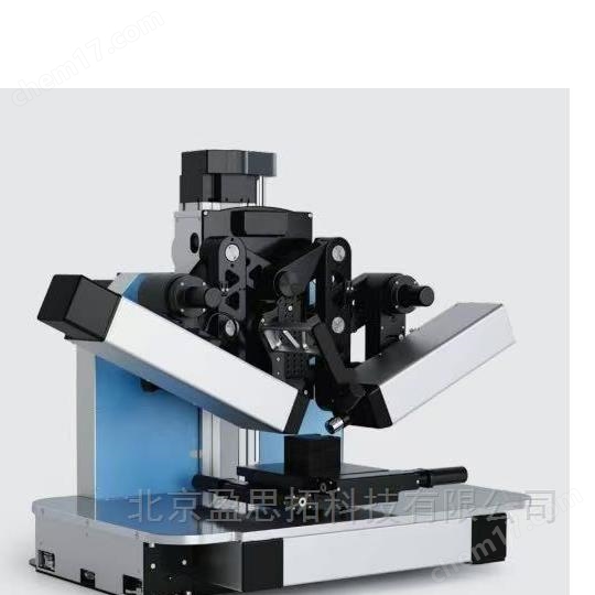


High resolution microscopy imaging ellipsometer
NegotiableUpdate on 02/06
- Model
- Nature of the Manufacturer
- Producers
- Product Category
- Place of Origin
Overview
This high-resolution microscopic imaging ellipsometer is different from traditional ellipsometers. It is a new generation of microscopic imaging ellipsometer technology that organically combines traditional spectral ellipsometer and optical microscope technology, allowing us to perform imaging ellipsometers as small as 1 The thickness and refractive index of the thin film are characterized by the sensitivity of an ellipsometer on the microstructure of m. The microscope is capable of simultaneously measuring all structures within the full field of view of the optical system.
Product Details
Unlike traditional ellipsometers, this is a new generation of microscopy imaging ellipsometer technology that combines organicallyTraditional spectroscopic ellipsometer and optical microscopeTechnology enables us to work on small things1 µ m microstructureThe sensitivity of the ellipsometer is used to characterize the thickness and refractive index of the thin film. The microscope part can measure simultaneouslyAll structures within the full field of view of the optical system.
Traditional ellipsometers focus on measuring the entire light spot, but cannot achieve high-precision lateral resolution and require point by point measurement. The microscope function of this device enables us to obtain microstructuresofElliptical enhanced contrast image,Small changes in refractive index or thickness can be seen in real-time images captured by the camera.Allow identification of the region of interest for ellipsometry measurement (selected measurement) to obtain values for thickness (0.1 nm-10 µ m) and refractive index.
You can connect this instrument withAtomic Force Microscopy (AFM), Quartz Crystal Microscopy (QCM-D), Reflectance Spectrometer, Raman SpectrometerBy combining other technologies, we can obtain more information from your samples.
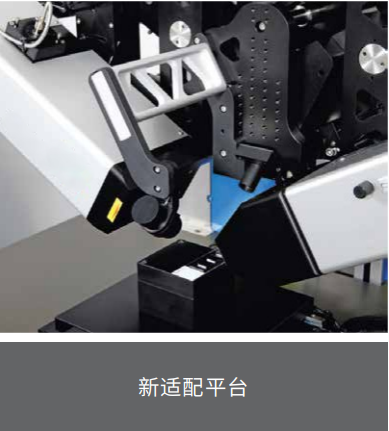
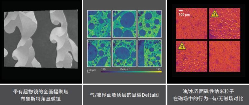
It is a modular instrument that can be configured differently according to your application direction. This instrument is equipped with a standard laser and can be used as a Brewster microscope, typically for the study of self-assembled monolayer LB films.
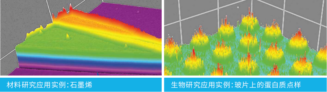
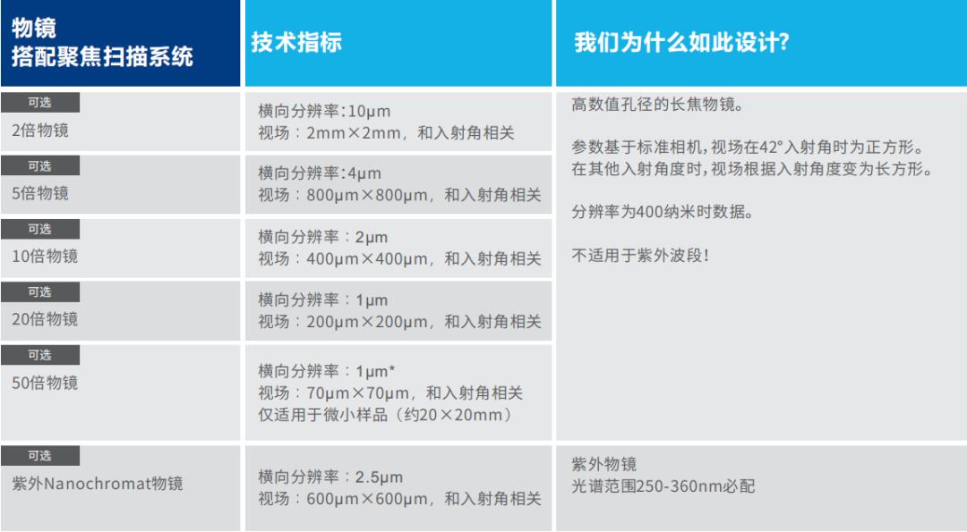
√ On the marketThe highest lateral ellipsoidal resolutionEllipsometer: capable of resolving1µmThis characteristic enables ellipsoidal analysis of microstructured and microscopic samples.
Real time ellipsoidal contrast imaging provides rapid image analysis of sample surfaces, various defects, or structures.
√ Selection analysis technologyPerform partial imaging analysis for regionalization (ROI).Parallel analysis technology enables synchronous analysis of multiple regions.
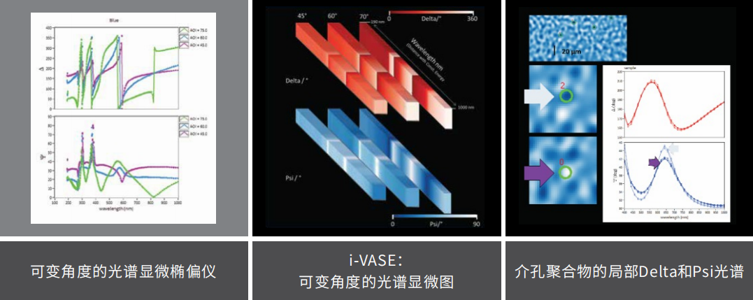
A spectral analyzer with a wavelength range of 190nm to 1700nm can provide micro ellipsometry analysis of samples over a wide wavelength range.
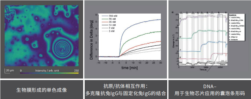
The optional full frame focusing technology (UltraObjective) in the visible light wavelength range is suitable for dynamic samples, such as the growth and movement of self-assembled monolayers, protein interactions, and drift measurement of monolayers on water surfaces.
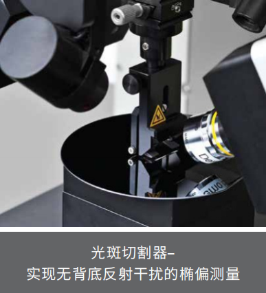
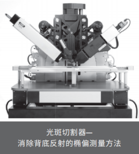
√ Spot cuttingTechnology, truly achieving thin films on ultra-thin transparent substratesNo back bottom reflectionElliptical polarization test.
√ Multiple functional extension attachments realize various practical functions of micro ellipsometry technology in different application fields, such as surface plasmon resonance (SPR), solid/liquid interface analysis unit, optical liquid/liquid interface analysis unit, microfluidic analysis unit, temperature control unit, electrochemical analysis unit, etc.
√ Microscopic ellipsometry analysis integrated platform, enabling the combination of multiple measurement techniques to obtain more information from your samples.
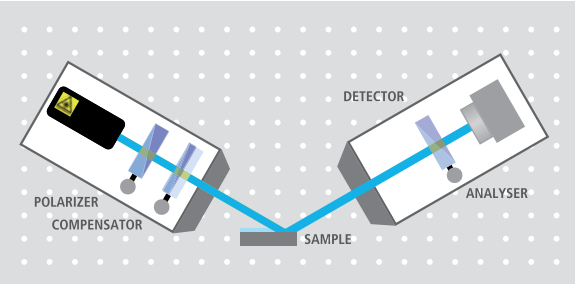
Elliptical polarization technology measures the reflection of a light beam passing through a thin filmPolarization stateAnalyze and obtain the property parameters of the tested film, and obtain parameter values (such as film thickness) that are even smaller than the wavelength of the probe light.
The properties of thin films, such as film thickness, refractive index, and absorption coefficient, are related to the changes in amplitude and phase of the p-component and s-component of the reflected beam.As the polarization component of the instrument rotates, the ellipsometer analyzes and measures the changes in amplitude and phase of the reflected beam, and the measurement data is the ellipsoidal Psi and Delta parameter values. Input these values into the computer and use simulation software for modeling and analysis, ultimately obtaining film property parameters such as film thickness, refractive index, and absorption coefficient. Other properties of the thin film, such as film structure, crystal properties, chemical composition, or conductivity, can be obtained through further analysis. Elliptical polarization has become a measurement methodMultilayer film thickness, refractive index, and absorption coefficientThe standard testing method.
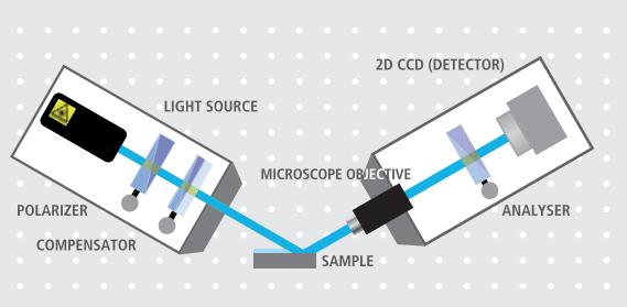
Microscopic ellipsometry technology is organically combinedExtinction ellipsometry technology and traditional microscopesTechnology, combined with microscope technology, allows you to perform measurements on the tested sampleVisual real-time image ellipsometry analysis,Horizontal (X/Y direction) resolution exceeding 1 µ m.
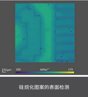
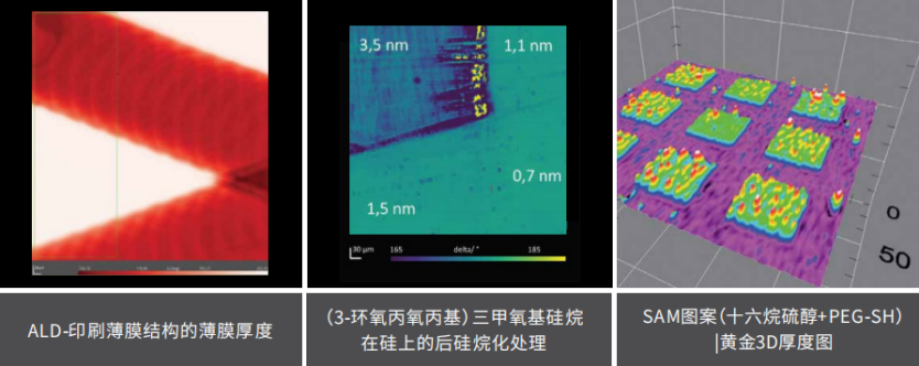
The minimum testing micro area of micro ellipsometry technology is one thousandth smaller than that of traditional micro spot ellipsometry, which can achieveRegionalization of non-uniform thin film specimensElliptical analysis. The selection analysis technology is used to achieve regional ellipsoidal analysis testing. Parallelization analysis technology allows you to perform synchronous analysis on multiple regions. passReal time video imagesAnalysis, microscopic ellipsometry technology can achieve manyIn situ surface interface analysisApplication. For example, micro ellipsometry technology is suitable for analyzing the surface and interface of thin films with lateral structural dimensions ranging from 1 um to 50 mm: patterned micro samples and thin films on micro cantilever sensors.The latest spot cutting technology can be used to achieve ellipsometry testing of thin films on transparent substrates without back bottom reflection interference.
The lateral resolution of a non microscopic ellipsometer is determined by the illumination of the sample surfacespot diameterdecision The diameter of the light spot varies from 35um to 2mm. The detection system detects the ellipsoidal state of the entire reflected beamPerform average ellipsometry analysis on all structures within the light spot rangeAll samples with microstructures smaller than this size cannot be accurately detected and analyzed. If your sample is not a uniform film, the averaging analysis test will yield incorrect data.
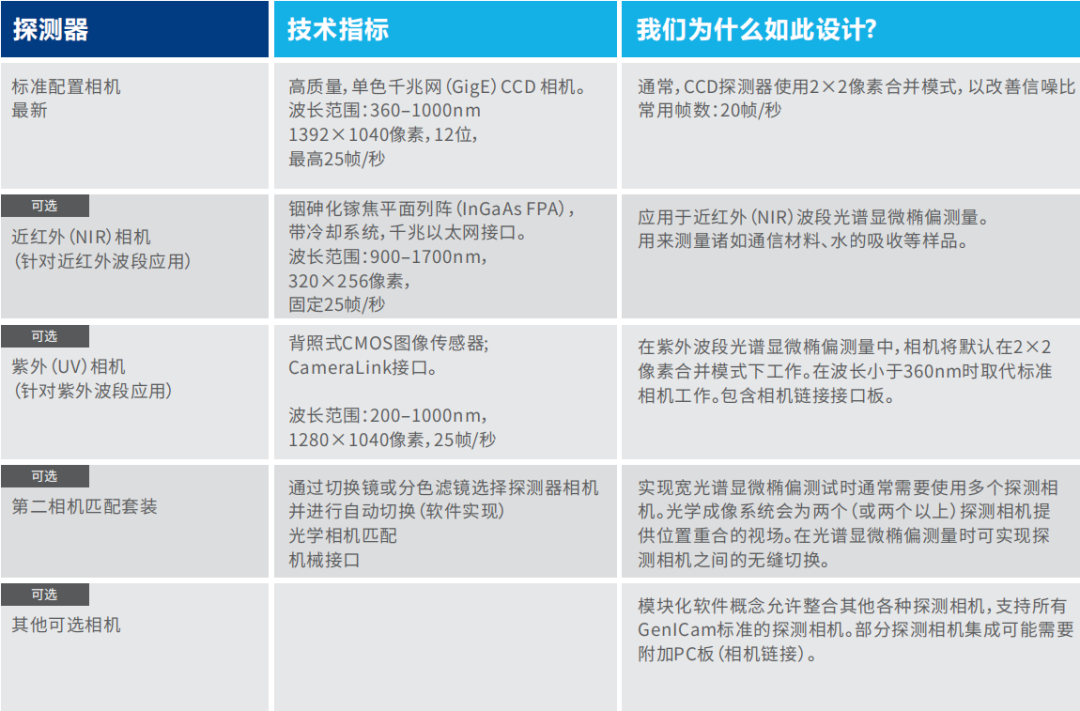
Microscopic ellipsometry techniqueHigh numerical aperture objective lens for sample imagingOn a high-resolution two-dimensional pixel detector arrayRealize million pixelsThe imaging. It provides a resolution as small as 1 micron,Specific resolution and wavelength related.

The sample stage mobile mapping ellipsometer is usually equipped with an electric sample stage, which measures Psi and Delta readings at one position point, then moves the sample stage to another position and repeats the process until sufficient data is collected to construct an imaging image of the sample surface. The lateral resolution is determined by the diameter of the light spot and the density of the selected measurement points. In addition to lower lateral resolution, sampling time is closely related to the number of sampling points. By comparison, optical microscopy (Imaging) ellipsometers canObtain up to millions of measurements in a single measurementAccording to,The horizontal resolution is much higher,And obtain Delta and Psi distribution maps. Compared with the sample stage moving ellipsometer, the optical microscope ellipsometer exhibits transverse ellipsometryThe resolution is much higher and the image acquisition time is much shorter.


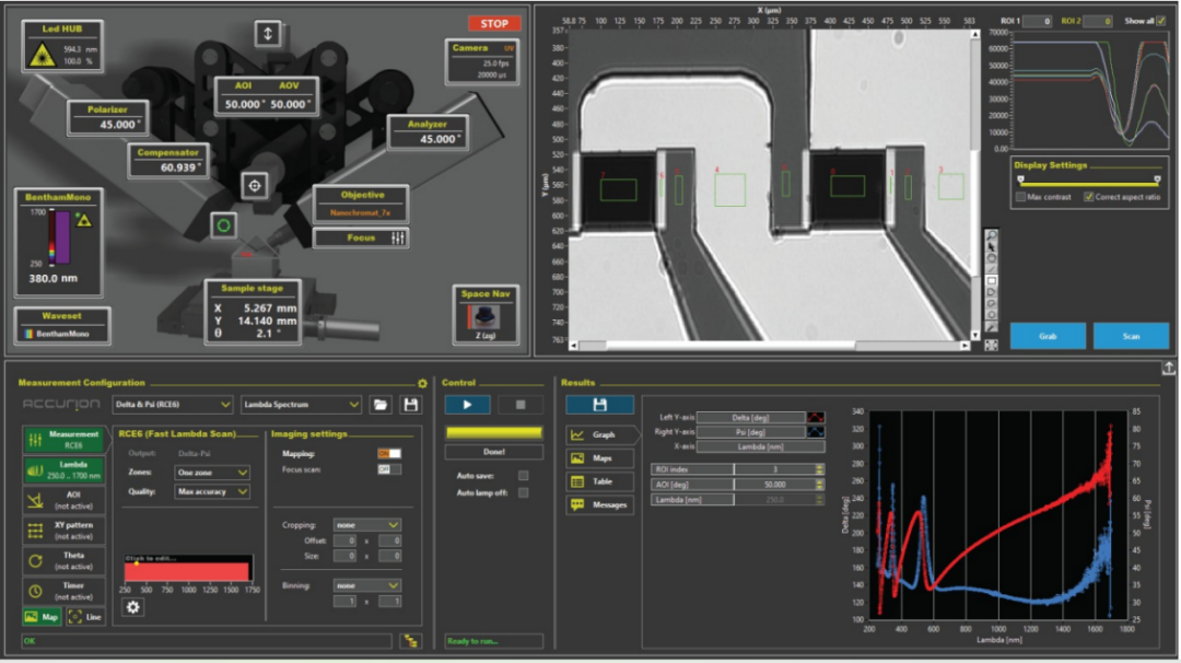
This device is equipped withModular softwareThe independent software module simplifies instrument operation and enables remote control measurement, data acquisition, and parallel or offline data analysis of the instrument.
The equipment control instrument control software manages the operation of the microscope analyzer equipment system.
It is an interactive and easy-to-use control software and automation tool.
The Server software manages and records all settings and data during the measurement process of the micro ellipsometer equipment, including parameter settings and data from various attachments and integrated systems. This is a data storage and analysis module that facilitates in-depth analysis and measurement of various complex samples.
Manage and store all relevant parameters and data, including parameters and measurement data of various attachments and associated systems.
Build a data storage structure for management (an easy-to-use structure).
√ Including image processing functionsBackground correction (motion correction), balance correction, visual correction, signal tracking (overall brightness correction), default test storage, and more functions.
Operating instruments (control of moving parts, capturing images, performing measurements, process automation, etc.)
Process all data (images, measurement results, kinematic tests, structural descriptions, etc.).
√ Independent of instruments, enabling offline data analysis and processing.
√ Special Features (Example):
1. Batch processing: Calculate the ellipsoidal data Delta/Psi and automatically convert it into a thickness distribution map (analyze pixel by pixel), automatically perform background correction.
2. All images, measurement data, and parameter information are stored continuously in real-time.

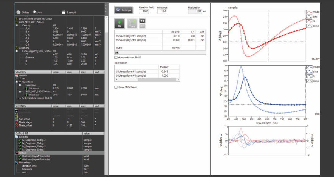
Use a large number of dispersion functions to analyze and fit measurement data.
Modeling of complex thin film systems and fitting measurement data using the selected model.
Simulate fitting to follow the effect of any parameters in the model.
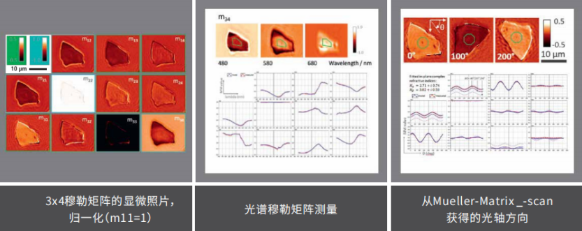
Modeling of refractive index (uniaxial, biaxial) and optical axis direction of anisotropic materials (based on 11 elements of normalized Mueller matrix).
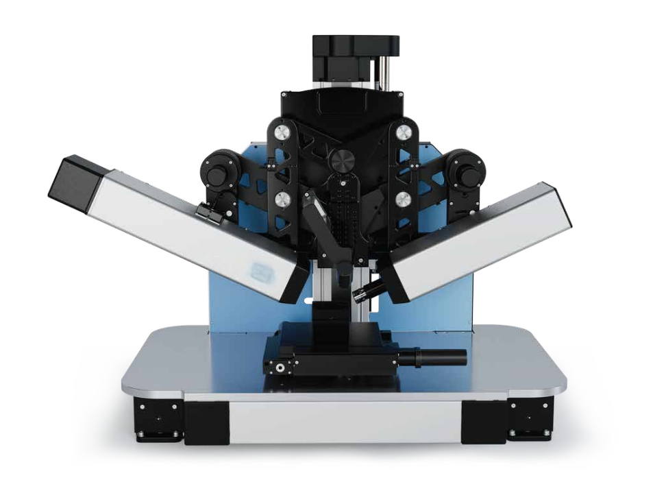
Microscopic ellipsometer, you can choose a configuration optimized for your measurement needs.


Similar Product Recommend


