-
E-mail
cindy_yst@instonetech.com
-
Phone
18600717106
-
Address
109-878, Building 20, No. 9 Antai Street, Konggang Street, Shunyi District, Beijing
Product Categories
Beijing Yingsitao Technology Co., Ltd


Frequency domain thermal reflection microscopy measurement system
NegotiableUpdate on 02/06
- Model
- Nature of the Manufacturer
- Producers
- Product Category
- Place of Origin
Overview
Equipment Introduction $r $n $r $n allows for multifunctional and innovative nanoscale thermal analysis $r $n $r $n √ Accurately evaluate the thermal conductivity of thin films and particles $r $n $r $n √ Use a three-dimensional diffusion model to reveal anisotropic thermal conductivity $r $n $r $n √ Quantify the thermal boundary thermal conductivity of deep interfaces $r $n $r $n √ Visualize thermal performance analysis at the microscale
Product Details
New Technology on the Market (FDTR)

Frequency domain thermal reflection microscopy measurement system
Introduction to Frequency Domain Heat Reflection Measurement System Equipment
Allow for multifunctional and innovative nanoscale thermal analysis
√ Accurately evaluate the thermal conductivity of thin films and particles
Using a three-dimensional diffusion model to reveal anisotropythermal conductivity
Quantify the thermal boundary thermal conductivity of deep interfaces
√ At the microscaleVisual thermal performance analysis
Basic principle: Frequency domain thermal reflection
What is heat reflection?
Heat reflection is the change of reflected light on the surface of a material relative to temperature.
When the temperature change is less than 10K, the heat reflection shows a linear change.
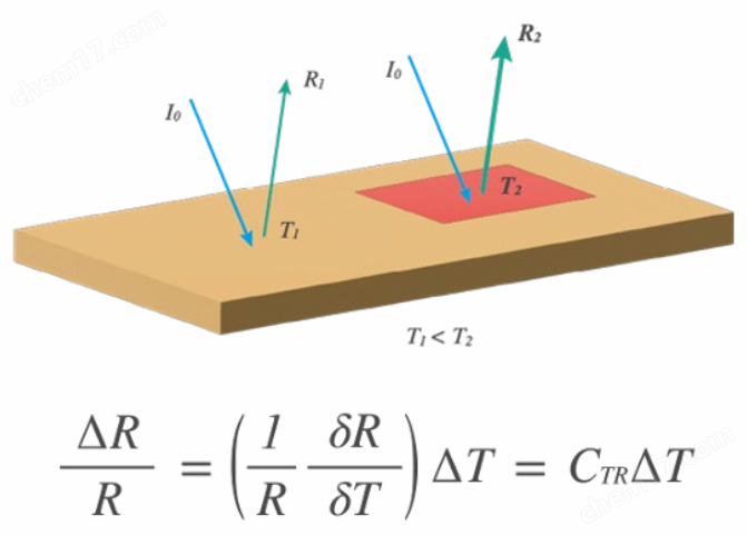
(CTR: Heat reflection coefficient)
Pump detection method for thermal reflection detection
The pump laser modulates at a specific frequency and periodically heats the surface of the sample. At the same time, the coaxial irradiation probe laser detects the phase delay in the thermal reflection signal of the thermal reflection component related to the surface temperature from the reflected probe light.

It is necessary to deposit a layer of gold converter on the surface of the sample to effectively convert pumped energy into heat and convert the resulting temperature changes into reflectivity changes
Phase delay in thermal reflection signal
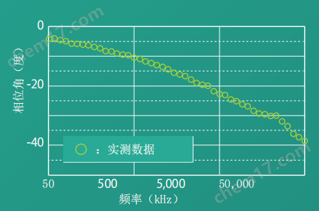
The heating signal and the heat reflection signal have the same frequency, but there is a phase delay between the two, which depends on the thermal physical properties and geometric shape of the sample.

Measurement of phase curve across frequencies
Scan the modulation frequency (heating frequency) of the pump laser from low to high and plot the phase delay curve, which can usually be obtained within 10 minutes.
Data fitting and parameter extraction
Thermophysical properties are quantitatively evaluated by fitting the obtained phase curve to a heat transfer model. The model includes the following parameters.
Parameters of each layer |
Cross plane and in-plane thermal conductivity (W/m · K), volumetric specific heat capacity (kJ/m ³)·K) And thickness (nm) |
Parameters inEach interface |
Thermal boundary thermal conductivity (MW/m2. K) |
The laser spot size and the offset distance between the pump laser and the detection laser are also included as fitting parameters

Main application areas of frequency domain thermal reflection measurement system
√semiconductor industryEvaluating the thermal boundary conductivity between the film and substrate, as well as the thermal conductivity of the heat dissipation filler particles, can be used for chip thermal failure analysis and electronic packaging material interface thermal conductivity assessment.
√Material development of thermoelectric convertersUsed to measure the thermal conductivity of thin films and small grains (through planes and interiors), in order to optimize the size of thermoelectric devices to the nanometer level to reduce thermal conductivity.
Part.1
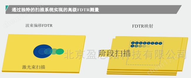
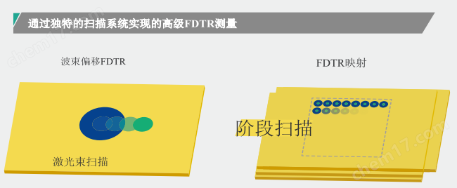
Functions achieved through laser scanning and micro focusing beams
By using microscale laser points and a three-dimensional thermal diffusion model, anisotropic thermal conductivity can be evaluated. The device is also capable of measuring thermal conductivity in microscale particles.

In addition to using electric platform scanning for FDTR mapping, laser beam scanning can also evaluate thermal conductivity and thermal boundary conduction within a plane.
Part.2
Breakthrough applications in the field of thermophysics
Thermal conductivity characterization
Block shaped substrates - sapphire and diamond
This case demonstrates the measurement of thermal conductivity on sapphire and diamond substrates. The fitting results show that the thermal conductivity of sapphire substrate is 30.8 W/m · K, while the thermal conductivity of diamond substrate is 2820.0 W/m · K. This indicates that even withtallMaterials with thermal conductivity can also be quantitatively evaluated.

Thin film - amorphous with a thickness of 100 nanometersGe1-xSnx
This study investigated the thermal conductivity of four amorphous germanium tin thin films with a thickness of approximately 100 nanometers deposited on a silicon substrate, which contain different concentrations of tin element. The results indicate that as the tin content increases, the thermal conductivity significantly decreases.

Characterization of Thermal Boundary Thermal Conductivity
Particles -18um single crystal alumina particles
The following chart shows a case study evaluating the thermal conductivity of single crystal oxide particles with a particle size of 18um. These particles have a rough/polyhedral structure, so we refine the thermal conductivity of the particles. These particles have a rough/polyhedral structure, so we refine the signal. The fitting results show that the thermal conductivity of these particles is comparable to that of bulk alumina.

Anisotropic material - bulk single crystal La5Ca9Cu24O41(LCCO)
This study revealed the bulk single crystal La by fitting the thermal conductivity by decomposing it into transverse and longitudinal components5Ca9Cu24O41The anisotropic thermal conductivity of LCCO materials. The results indicate that due to the magnon effect, its transverse thermal conductivity is relatively high; The lower longitudinal thermal conductivity is mainly due to phonon effects.

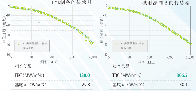
Thermal Boundary Thermal Conductivity - PVD and Sputtering
By comparing experimental data, we revealed the variation of thermal boundary conductivity (TBC) at the sapphire substrate interface when preparing gold substrates using physical vapor deposition (PVD) and sputtering processes. Experimental data shows that the TBC value under PVD process is 138.0 MW/m2·K. And the sputtering process reaches 306.5 MW/m2·K. The thermal conductivity of the substrate is similar in both processes.
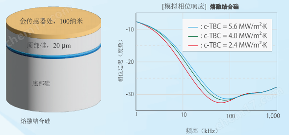
Thermal boundary thermal conductivity - melt bonded silicon interface
A simulation study investigated whether FDTR can detect changes in the composite thermal boundary thermal conductivity (c-TBC) at the fusion bonded silicon wafer interface - a parameter that comprehensively reflects the combined effect of multiple dielectric layers and the interface at the molten silicon wafer interface. Assuming c-TBC is 4.0MW/m2·K with a fluctuation amplitude of ± 40% and a beam diameter of 50um, the results show that effective measurement data can be obtained in the low-frequency range of 10-50 kHz for silicon layers with a thickness of less than 20um.
Similar Product Recommend


