-
E-mail
sende_services@outlook.com
-
Phone
17688459448
-
Address
No. 983 Huangpu Avenue East, Huangpu District, Guangzhou City, Guangdong Province
Product Categories
Guangdong Sende Instrument Co., Ltd
Field emission scanning electron microscope
NegotiableUpdate on 02/08
- Model
- Nature of the Manufacturer
- Producers
- Product Category
- Place of Origin
Overview
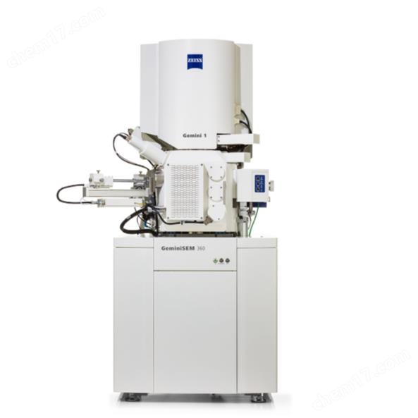
GeminiSEM 360 can help you easily achieve sub nanometer resolution imaging. Excellent imaging and analysis techniques further enhance FE-SEM (Field Emission Scanning Electron Microscopy).
Product Details
Zeiss GeminiSEM 360
FE-SEM meets the high requirements for sub nanometer imaging, analysis, and sample flexibility
Zeiss GeminiSEM can help you easily achieve sub nanometer resolution imaging. Excellent imaging and analysis techniques further enhance FE-SEM(Field emission scanning electron microscope)Like adding wings to a tiger. We adopt innovative electronic optical systems and a brand new sample chamber design, which not only makes operation easier and usage more flexible and diverse, but also brings you higher image quality. Sub nanometer level images below 1 kV can be captured without immersion of the objective lens in water. Explore three designs of Zeiss Gemini electro-optical system:
lIdeal choice for analysis and testing platform——Zeiss GeminiSEM 360
lRealize efficient analysis——Zeiss GeminiSEM 460
lNew standards for surface imaging——CaiGeminiSEM 560

GeminiSEM 360(Field emission scanning electron microscope)It is an ideal device for your analysis and testing platform, providing beneficial functionality for materials and life sciences, as well as industrial fields. With its Gemini1 electron optical tube, GeminiSEM 360 can provide high-resolution imaging and analysis for various applications and sample types.
✔High sample flexibility
✔Excellent user experience
✔Outstanding expansion ability


High sample flexibility
✔ GeminiSEM 360 is an ideal device for analyzing and testing platforms, providing beneficial functionality for materials and life sciences, as well as industrial fields.
✔ The Gemini 1 electron optical design of the same name provides surface sensitive high-resolution images, with excellent resolution even under low voltage conditions and fast imaging under high probe current conditions.
✔ Inlens secondary electron imaging and backscattered electron imaging can simultaneously collect high-resolution surface morphology and composite composition contrast information (the same applies to electron beam sensitive samples).
✔ When imaging insulating samples under low vacuum conditions (i.e. variable pressure), there is no need to sacrifice Inlens contrast: NanoVP ensures outstanding functionality, ensuring Inlens imaging without being affected by electric charges.

Excellent user experience
✔ GeminiSEM 360 brings a great user experience: with its wide observation field and highly personalized new sample compartment, it can easily detect even when facing ultra large samples.
✔ The correlation imaging and correlation microscopy technology achieved through Zeiss ZEN Connect allows you to enjoy seamless navigation.
✔ Use automatic functions such as autofocus and smart detectors to easily obtain clear images.
✔ The geometrically symmetrical design of EDS ports and the coplanar EDS/EBSD geometry structure make it easier for you to perform efficient imaging and analysis workflows.
✔ Zeiss Predictive Service allows you to fully utilize system runtime and enjoy the advantages of regular maintenance at any time.

Outstanding expansion ability
✔ The continuous upgrading of the system is a prerequisite for ensuring your investment. Therefore, GeminiSEM 360 is also a member of the Zeiss ZEN core software ecosystem, allowing you to enjoy the convenience of system upgrades.
✔ ZEN Connect can combine multimodal and multi-scale data, ZEN Intellesis is used for image segmentation supported by advanced artificial intelligence, ZEN's analysis module is used to report and analyze segmented data, and ZEN data storage allows you to centrally manage projects by connecting data collected from different devices in the laboratory.
✔ As a member of the APEER community, you can access workflows and scripts created by other users to remotely help you solve problems.
✔ Due to providing a clear upgrade path, the system can be further improved with the release of new features.
Introduction to Basic Principles
FE-SEM is designed specifically for high-resolution imaging, and a key performance factor is its electron optical tube. Gemini is specially designed to achieve excellent resolution for any sample (especially at low acceleration voltages), enabling complete and efficient detection with simple operation.

The Gemini electron optical system has the following three main characteristics:
The design of Gemini objective combines electrostatic and electromagnetic fields, greatly improving optical performance while significantly reducing the impact on the sample. This can also achieve high-quality imaging of challenging samples such as magnetic materials.
Gemini electron beam thruster technology is an integrated beam reducer that ensures small-sized electron beam spots and high signal-to-noise ratio.
The detection design principle of Gemini Inlens significantly reduces the time to image by simultaneously detecting secondary electrons (SE) and backscattered electrons (BSE), ensuring efficient signal detection.

For your application, there are the following advantages:
✔ SEM electron beam alignment can maintain stability for a long time, and changing the probe current and acceleration voltage has almost no effect on the system.
✔ An optical system with almost no magnetic field leakage can achieve distortion free high-resolution imaging.
✔ By using the Inlens SE detector, images can be generated using true surface sensitivity SE 1 electronic technology, allowing only the top-level information of the sample to be obtained.
✔ The detection design concept of using Inlens EsB detector achieves true material composition contrast at very low voltages.


Similar Product Recommend