-
E-mail
michael.han@sypht.com.cn
- Phone
-
Address
Wujiang District Science and Technology Innovation Park, Suzhou City, Jiangsu Province
Product Categories
Saifei Scientific Instruments (Suzhou) Co., Ltd

Field emission scanning electron microscope
NegotiableUpdate on 01/30
- Model
- Nature of the Manufacturer
- Producers
- Product Category
- Place of Origin
Overview
The JSM-IT810 $r $n field emission scanning electron microscope $r $n JSM-IT810 series FE-SEM combines multifunctionality and high spatial resolution to achieve automated operation. Built in imaging and EDS analysis automation functions that do not require coding, making the workflow smoother and more efficient. In addition, some new features have been added to ensure that all SEM users receive high-quality data and a better user experience. The operation of FE-SEM has never been as simple as the JSM-IT810 series.
Product Details
JSM-IT810Field emission scanning electron microscopeBy utilizing automation technology, the operational efficiency from instrument debugging to observation and analysis has been improved!
JSM-IT810Field emission scanning electron microscopeThe FE-SEM series combines multifunctionality and high spatial resolution to achieve automated operations. Built in imaging and EDS analysis automation functions that do not require coding, making the workflow smoother and more efficient. In addition, some new features have been added to ensure that all SEM users receive high-quality data and a better user experience. These features include SEM automatic adjustment package, trapezoidal correction function (very useful in EBSD testing), and Live 3D reconstruction function for observing surface morphology.
The operation of FE-SEM has never been as simple as the JSM-IT810 series.
Main features
1. Automatic observation and analysis function "Neo Action"
Intelligent operation, automatic execution of SEM observation and energy dispersive spectroscopy (EDS) analysis

Sample: Chondrules in chondrite Julesberg (L3.6),Landing Voltage: 5 kV
2. Automatic calibration function "SEM automatic adjustment package"
Use standard samples for automatic magnification adjustment, electron beam alignment, and EDS energy calibration. Regularly inspect to ensure that the equipment is in good condition.

3. Real time 3D functionality
The 5-segment semiconductor detector can choose backscattered electron signals. The two-dimensional images obtained from the outer four segments can be used for three-dimensional image reconstruction.
The new Live-3D feature enables real-time measurement and inspection of the topology structure of samples.

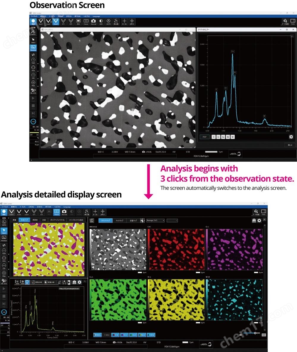
4. Integrated EDS
The integrated EDS eliminates the barriers between SEM observation and EDS elemental analysis. Observing various analysis modes such as dots, faces, lines, and MAP on the screen allows for immediate analysis.
Similar Product Recommend


