-
E-mail
huangjin@fsm-sz.cn
-
Phone
18934598975
-
Address
JD.com, Wuzhong District, Suzhou City The Taihu Lake Intelligent Manufacturing Industrial Park (No. 7, Longshan South Road) 3A # 401-402
Product Categories
Suzhou Feishiman Precision Instrument Co., Ltd

atomic force microscope
NegotiableUpdate on 01/12
- Model
- Nature of the Manufacturer
- Producers
- Product Category
- Place of Origin
Overview
Atomic force microscopy is a powerful nanoscale characterization tool that reconstructs the three-dimensional surface morphology by sensing the extremely weak interaction between the probe and the sample. Its advantages lie in high resolution, three-dimensional imaging capability, and the ability to study samples under close to natural conditions (especially in liquids), making it the "eye" and "hand" in the fields of materials science, life sciences, and nanotechnology.
Product Details
1、 What is an atomic force microscope?
Atomic force microscope is a type of ultra-high resolution scanning probe microscope with nanometer or even atomic level resolution. Its core principle is very simple: sensing the three-dimensional morphology and physical properties of the sample surface by gently "touching" or scanning it with an extremely fine probe.
The most amazing thing is that AFM does not need to work in a vacuum environment like an electron microscope, it can operate in atmospheric, liquid, and even vacuum environments. This enables it to observe biological macromolecules (such as proteins, DNA), live cells, and other samples that cannot be directly observed under an electron microscope, which is a huge advantage of it.
2、 Working principle
The working principle of AFM is similar to that of ancient record players, where the stylus reads grooves on a record, but the accuracy is countless orders of magnitude higher. Its core components include:
1. Micro cantilever beam: a highly elastic micro cantilever.
2. Probe: an extremely sharp needle tip located at the end of a cantilever beam, with a curvature radius of up to the nanometer level.
3. Laser emission and position detection system: A laser beam is directed onto the back of a cantilever beam and reflected onto a four quadrant photodetector.
4. Piezoelectric scanner: a ceramic material capable of achieving nanometer level precise positioning, which can control the probe or sample to move accurately in the X, Y, and Z directions.
Work process (taking contact mode as an example):
1. Contact: Gradually approach the sharp probe to the surface of the sample until it generates weak interaction forces (mainly van der Waals forces) with the atoms on the sample surface.
2. Scanning: The piezoelectric scanner drives the probe to perform line by line scanning (grid scanning) on the surface of the sample.
3. Perceived deformation: When the probe scans areas with surface undulations, the force between the needle tip and the sample changes, causing the microcantilever beam to bend (deform).
4. Detecting deformation: The bending of the cantilever beam will change the direction of the reflected laser beam, resulting in a change in the position of the light spot on the photodetector. This positional change is accurately recorded.
5. Feedback loop: The system adjusts the height of the piezoelectric scanner in the Z direction in real-time through a feedback loop to maintain constant deformation of the cantilever beam (i.e. the force between the probe and the sample).
6. Imaging: The computer records the Z-direction height change required for the scanner to maintain a constant force at each point (X, Y coordinates). By combining these data, a three-dimensional morphology map of the sample surface is obtained.
3、 Main working mode
AFM has multiple working modes to adapt to different samples and measurement needs, mainly divided into three categories:
1. Contact mode
Principle: The probe is in direct contact with the sample surface (repulsive mode), and the distance between the cantilever beam and the sample surface is less than a few nanometers.
Advantages: High resolution and fast scanning speed.
Disadvantage: Lateral forces may cause damage or movement to soft samples, such as biological samples.
2. Tap mode
Principle: Make the microcantilever beam oscillate near its resonance frequency, and the probe only briefly "taps" the sample surface at the bottom of each oscillation cycle. Feedback surface morphology by detecting changes in oscillation amplitude.
Advantages: It greatly reduces lateral force and is very suitable for observing soft, fragile, or highly adhesive samples (such as biological and polymer materials), making it one of the widely used modes.
Disadvantage: Scanning speed is slightly slower than contact mode.
3. Non contact mode
Principle: The probe vibrates above the surface of the sample (at a distance of several tens of nanometers), and images by detecting changes in long-range forces (such as van der Waals forces and electrostatic forces) between the sample and the needle tip.
Advantages: Almost zero damage to the sample.
Disadvantages: Low resolution, usually requiring operation in a vacuum environment to eliminate interference from air damping.
4、 Main application areas
The powerful functions of AFM make it applicable in many fields:
1. Materials Science:
Observe the morphology and structure of nanomaterials such as graphene and carbon nanotubes.
Study the surface roughness, grain boundaries, and defects of materials such as metals, semiconductors, and ceramics.
Analyze the phase separation and crystal structure of polymer materials.
2. Life Sciences and Biology:
Imaging: Directly observing the structure of biomolecules such as DNA, RNA, proteins, and even the dynamic changes of biological processes in liquid environments.
Mechanical property measurement: Through force curve measurement, study the elasticity (stiffness) of living cells, bacterial adhesion, protein-protein interactions, etc.
3. Nanotechnology:
Nanomanipulation: Moving individual atoms or molecules to construct nanostructures.
Nanoprocessing: Using AFM tips to etch and oxidize the surface of materials, achieving "direct writing" processing.
4. Semiconductor industry:
Measure the line width and depth of integrated circuits for failure analysis.
Detect the surface quality of semiconductor devices.
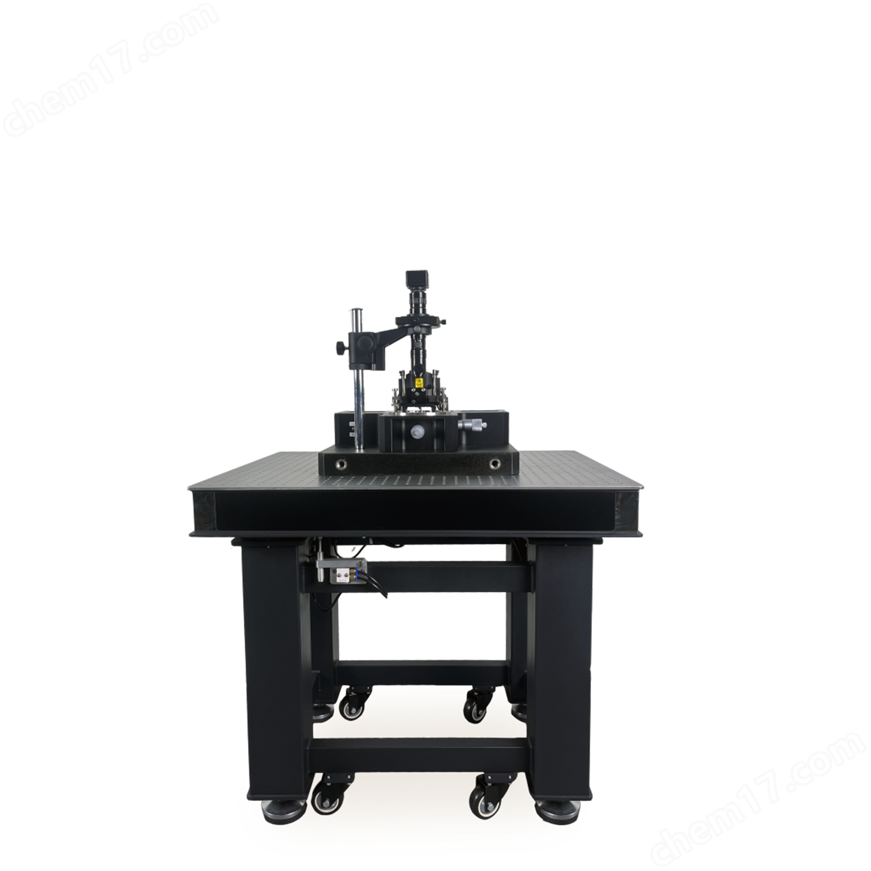
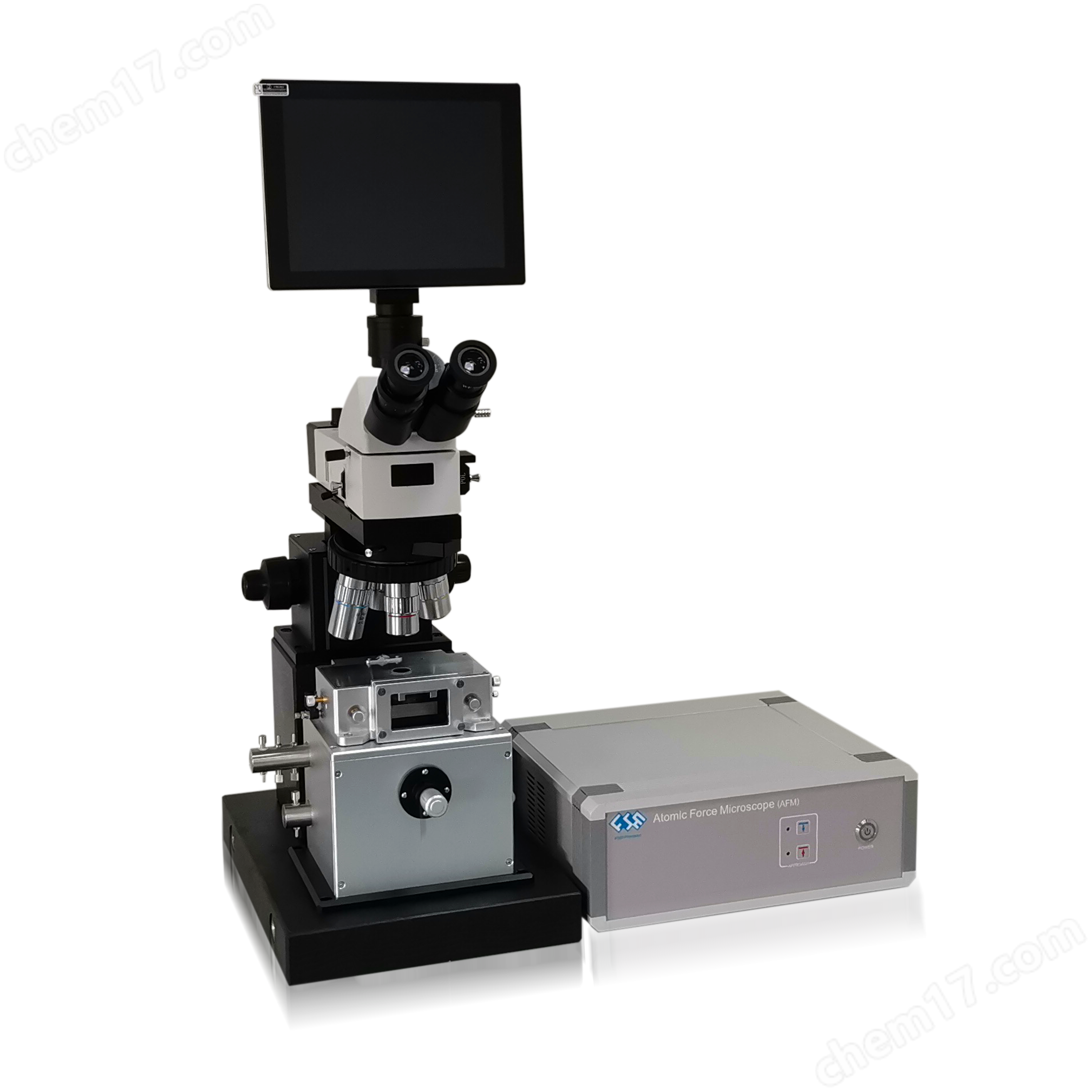
The laser detection head and sample scanning table are integrated into one, stable and reliable;
Precision laser and probe positioning device, easy and convenient to replace probes and adjust light spots;
◆ Single axis drive sample automatically approaches the probe vertically, accurately locates the scanning area, and makes the needle tip perpendicular to the sample during scanning;
Intelligent needle insertion method for motor controlled pressurized ceramic automatic detection, protecting probes and samples;
High precision and wide range piezoelectric ceramic scanner, which can be selected according to different precision and scanning range requirements;
High precision and wide range piezoelectric ceramic scanner, which can be selected according to different precision and scanning range requirements;
10X apochromatic objective lens optical positioning, no need for focusing, real-time observation.
6、 Atomic force microscopeTechnical Specifications:
| Basic working mode | Contact mode, tap mode, F-Z force curve measurement, RMS-Z curve measurement |
| Optional working mode | Friction/lateral force, amplitude/phase, magnetic force, and electrostatic force |
| sample size | Φ≤90mm,H≤20mm |
| scanning range | XY direction 50um, Z direction 5um (optional XY direction 110um, Z direction 10um) |
| Scanning resolution | XY direction 0.2nm, Z direction 0.05nm |
| Sample movement range | 0~20mm |
| Optical magnification factor | 10X, Optical resolution of 1um (optional 20X, optical resolution of 0.8um) |
| scan rate | 0.6Hz~4.34Hz, Scanning angle 0~360 ° |
| scan control | XY uses 18 bit D/A, Z uses 16 bit D/A |
| Data sampling | 14-bit A/D、 Dual 16 bit A/D multi-channel synchronous sampling |
| Feedback method | DSP digital feedback |
| Feedback sampling rate | 64.0KHz |
| communication interface | USB2.0/3.0 |
| runtime environment | Windows XP/7/8/10 operating system |