-
E-mail
info@giantforce.cn
-
Phone
18911365393
-
Address
1311, Building B, Wanda Plaza, No. 58 Xinhua West Street, Tongzhou District, Beijing
Product Categories
- High power laser material tester
- Steady-state solar simulator
- Laser beam analyzer
- High power laser beam analyzer
- Desktop laser direct writing system
- Large Spot Laser Beam Analyzer
- Desktop Maskless Lithography System
- QFLS Quasi Fermi Level Splitting Tester
- Absolute PL Quantum Yield Testing System
- Solar cell PL imaging system
- Solar cell iVoc imaging system
- Solar panel PL imaging system
Juli Optoelectronics (Beijing) Technology Co., Ltd

QFLS Quasi Fermi Level Splitting Tester
NegotiableUpdate on 12/16
- Model
- Nature of the Manufacturer
- Producers
- Product Category
- Place of Origin
Overview
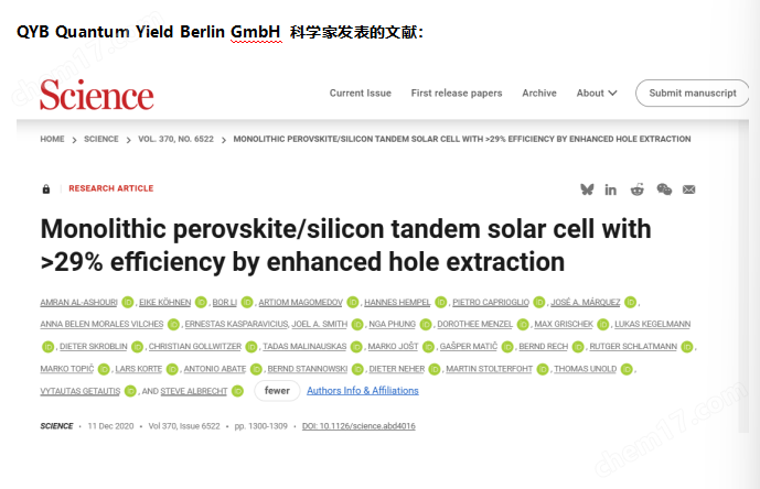
The QFLS quasi Fermi level splitting tester was developed by scientists from QYB Quantum Yield Berlin GmbH, a spin off company of the Helmholtz Center (HZB) in Berlin, Germany. The team set a century record of 29.15% efficiency for perovskite/silicon stacked solar cells in 2020, and the corresponding article was published in Science (DOI: 10.1126/science. abd4016).
Product Details
QFLS Quasi Fermi Level Splitting Tester
(Quasi-Fermi Level Splitting Tester)
QFLS Quasi Fermi Level Splitting TesterDeveloped by scientists from QYB Quantum Yield Berlin GmbH, spin off by the Helmholtz Center (HZB) in Berlin, Germany.The team set a century record of 29.15% efficiency for perovskite/silicon stacked solar cells in 2020, and the corresponding article was published inScienceUp there(DOI: 10.1126/science.abd4016).
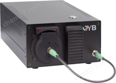
Used to test the absolute electroluminescence spectra and photoluminescence spectra of photovoltaic devices such as solar cells and LEDs, and calculate the iVoc implied open circuit voltage, EL/PLKY quantum yield, QFLS quasi Fermi level splitting, etc. The device is designed to be compact, easy to operate, and can be placed inside a glove box.
l
Technical features:
ELQY/PLKY sensitivity ≥ 1E-6
*ELQY electroluminescence quantum yield,
*PLQY photoluminescence quantum yield
Absolute luminous flux measurement
Absolute EL/PL spectrum detection
Direct EL/PLKY quantum yield calculation
Direct QFLS quasi Fermi level splitting calculation
Ideal factor calculation
Pseudo JV construction
Laser intensity scanning measurement
Electrical bias scanning measurement
Automatic continuous laser intensity adjustable from 0.001 to 10 "suns"
Bias current/voltage function
Integrated SMU

l softOperation interface:
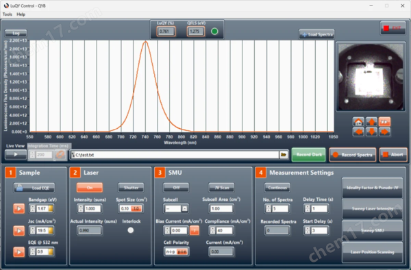
The software displays the luminescence spectrum of the measured sample under various excitation conditions.
*Upper window: Display the emission spectrum, camera field of view, and calculate the values of LuQY (ELQY/PLQY) and QFLS.
*Lower window: Sample information(“1” -increaseQFLS calculation credibility)Adjust excitation and testing settings(“2” – “4”).
The software adopts two QFLS quasi Fermi level splitting calculation methods and automatically selects the highly reliable method for each measurement. This can depend on the emission type (e.g. wide bandgap emission) and whether the user provides light absorption data.
l Direct QFLS quasi Fermi level splitting prediction:
-Not requiring specified data for samples, low credibility
-Reliable QFLS quasi Fermi level splitting prediction for low bandgap emission and lowStokes displacementlaunch
l Fine QFLS quasi Fermi level splitting prediction:
-Provide sample specific absorption data to increase the credibility of QFLS quasi Fermi level splitting
-Optical bandgap, short-circuit current density Jsc@STC The quantum efficiency of EQE at 532nm can be manually inputted or extracted from EQE/absorption spectra
-Providing sample data can achieve set point excitation settings (such as 1sun equivalent laser excitation) and improve the accuracy of QFLS quasi Fermi level splitting prediction.

l System resolution capability

a) Extreme laser intensity with spot sizes of 0.1 and 1cm respectively2Next, the optical bandgap of the sample (assuming ideal absorption of the sample and photon energy below)0, the energy above the optical bandgap is 1)
b) LuQY (EL/PLKY) optical bandgap energy can be resolved (assuming: a) ideal absorption of the sample, emission Stokes shift of 0, dashed line represents LuQY resolution @ different excitation intensities, spot sizes of 0.1 and 1cm2.
l Technical Specifications
Photon excitation wavelength:532 nm
Ultimate laser power:140 mW
Adjustable photon excitation intensity (equivalent current):4 μA to 40 mA
Photon excitation spot (optional):0.1 cm² / 1 cm²
Spectral measurement range:550 - 1050 nm
Lower limit distinguishable luminescence quantum yield:1E-6
Integral time:1 ms – 35 min
Spectral sampling interval:1 nm
Signal to Noise Ratio:600:1
Current voltage source and measuring unit:±10 V, ±150 mA
Voltage source accuracy:10 mV
Voltage induction accuracy:50 μV
Current induction accuracy:100 nA, 1 μA, 10 μA
Sample fixture: customizable (sample size)30mmX30mmX10mm)
Number of test sub samples:6 subcells
Equipment size:220 mm x 390 mm x 120 mm
Weight:6.1 kg
Note:LuQY Pro laser intensity calibration based on absolute photon countcertified reference solar cells from Fraunhofer ISE CalLab PV Cells.The spectral sensitivity calibration of LuQY Pro is based on the absolute photon number, which can be traced back to the known luminous flux of NIST lamps.

References:
Publications Using LuQY Pro/LuQYMeasurement System
[1]
L. Jiaet. al., „Efficient perovskite/silicon tandem with asymmetric self-assembly molecule“,Nature, July 2025, doi:10.1038/s41586-025-09333-z.
[2]
Z. Jiaet al., “Efficient near-infrared harvesting in perovskite–organic tandem solar cells,”Nature, vol. 643, no. 8070, pp. 104–110, Jul. 2025, doi:10.1038/s41586-025-09181-x.
[3]
H. Chenet al., “Improved charge extraction in inverted perovskite solar cells with dual-site-binding ligands,”Science, vol. 384, no. 6692, pp. 189–193, Apr. 2024, doi:10.1126/science.adm9474.
[4]
J. Liet al., “Enhancing the efficiency and longevity of inverted perovskite solar cells with antimony-doped tin oxides,”Nature Energy, vol. 9, no. 3, pp. 308–315, Mar. 2024, doi:10.1038/s41560-023-01442-1.
[5]
Z. Weiet al., “Surpassing 90% Shockley–QueisserVOClimit in 1.79 eV wide-bandgap perovskite solar cells using bromine-substituted self-assembled monolayers,”Energy Environ. Sci., vol. 18, no. 4, pp. 1847–1855, 2025, doi:10.1039/d4ee04029e.
[6]
X. Tangetal., „Enhancing the efficiency and stability of perovskite solar cells via a polymer heterointerface bridge“,Nat. Photon., June 2025, doi:10.1038/s41566-025-01676-3.
[7]
Y. Yuan, G. Yan, S. Akel, U. Rau, and T. Kirchartz, “Deriving mobility-lifetime products in halide perovskite films from spectrally- and time-resolved photoluminescence,” Apr. 16, 2025,Science Advances. doi:10.1126/sciadv.adt1171.
[8]
E. Alviantoet al., „Industry‐Compatible Fully Laminated Perovskite‐CIGS Tandem Solar Cells with Co‐Evaporated Perovskite“,Advanced Materials, July 2025, doi:10.1002/adma.202505571.
[9]
O. Er-rajiet al., “Tailoring perovskite crystallization and interfacial passivation in efficient, fully textured perovskite silicon tandem solar cells,”Joule, vol. 0, no. 0, Jul. 2024, doi:10.1016/j.joule.2024.06.018.
[10]
H. Lianget al., “29.9%-efficient, commercially viable perovskite/CuInSe2 thin-film tandem solar cells,”Joule, vol. 7, no. 12, pp. 2859–2872, Dec. 2023, doi:10.1016/j.joule.2023.10.007.


