-
E-mail
Wayne.Zhang@Sikcn.com
-
Phone
13917975482
-
Address
7th Floor, Building 7, Zhangjiang Microelectronics Port, No. 690 Bibo Road
Product Categories
Tiankong Scientific Instruments (Shanghai) Co., Ltd
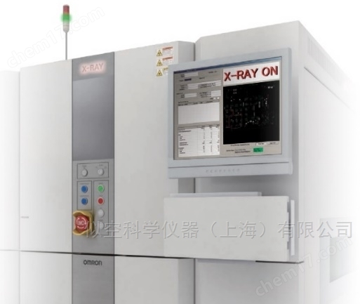


OMRON High Speed Automated 3D-CT Inspection System (AXI)
NegotiableUpdate on 01/13
- Model
- Nature of the Manufacturer
- Producers
- Product Category
- Place of Origin
Overview
As a high-speed and high-quality inspection device using full 3D-CT, VT-X750 is widely used for non-destructive inspection of 5G infrastructure/modules and on-board electrical components, as well as in aerospace, industrial equipment, semiconductor and other fields. In recent years, this model has been used for inspecting power devices such as IGBT and MOSFET in electric vehicles, internal bubbles in soldering of mechatronics products, and soldering filling of through-hole connectors.
Product Details
As a fully adoptedThe high-speed and high-quality inspection device of 3D-CT, VT-X750, is widely used for non-destructive inspection of 5G infrastructure/modules and on-board electrical components, as well as aerospace and industrial applicationsIndustries such as equipment and semiconductors. In recent years, this model has been used for electric vehiclesInternal bubbles and through holes in the solder of power devices such as IGBT and MOSFET, as well as mechatronics productsInspection of solder filling and other related aspects of connectors
Applicable products:
BGA/CSPInsert componentsSOP/QFPTransistorsR/CChips, bottom electrode componentsQFNPower modulePOPThepress-fitConnectors, etc
Inspection items:
Bubbles, open soldering, non wetting, solder quantity, offset, bridging, solder crawling, through-hole solder filling, solder beads, etc(Can be selected based on the inspection object)
core value:
✓ OnlineFull board high-speed scanning
Industry leaders3D-CT technology, realizing whole board components (including BGA/connectors/chips, etc.)online100% non-destructive testing, with a speed comparable to previous generation models(VT-X700)More than twice→Full inspection of M-sized substrates only takes minutes (including 2000+pins BGA/SiP)
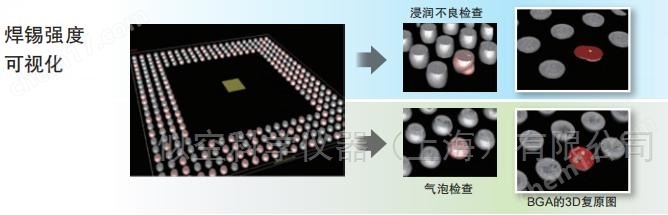
✓Visualization of solder strength
Du HomeThe 3D-CT algorithm accurately quantifies the shape of solder, achieving:
•Solder bubbles/Virtual soldering/bridging/tin crawling, etcMicron level defect detection
•Quick quality verification during production switching to eliminate design constraints
✓AI intelligent assistance system |
✓ Safety zero stop line guarantee |
• Automatic judgmentOK/NG (AI+quantitative double standard) |
Radiation reduction technology (standard filter)+High speed scanning |
Intelligent generation detection program(Automatic Conversion of CAD Data |
• Component radiation simulator predicts risks |
• Optimal parameter simulation (beat)/Radiation adaptive optimization) |
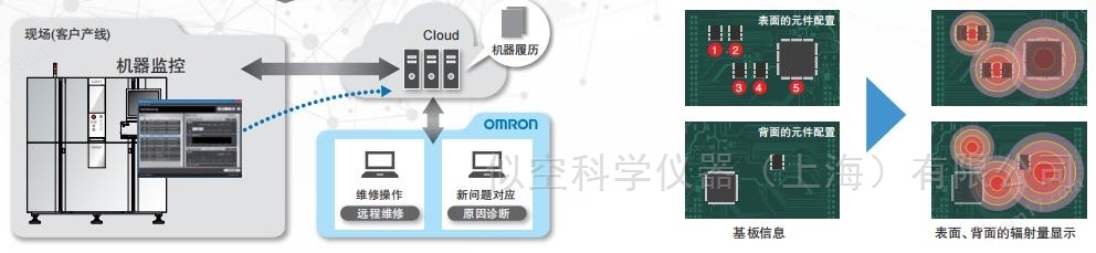
Global remote monitoring support |
Technical specifications:
project |
content |
|||
model |
VT-X750 |
VT-X750-XL |
||
type |
V3-H |
V3-C |
V2-H |
|
Shooting resolution |
6~30μ m adjustable |
6~30μ m adjustable |
10~30μ m adjustable |
|
Object substrate |
Substrate size |
50×50~610×515mm Thickness0.4~5.0mm (resolution3μmtime0.4~3.0mm) |
100×50~1200×610mm Thickness0.4~15.0mm |
|
Substrate weight |
4.0kgBelow8.0kgbelow(※ Options) |
15kgbelow |
||
warp |
2.0mmbelow(resolution3μmtime1.0mmbelow) |
3.0 mmbelow |
||
Similar Product Recommend