- Phone
-
Address
No. 5500 Yuanjiang Road, Minhang District, Shanghai
Product Categories
Shanghai Maikewei Semiconductor Technology Co., Ltd
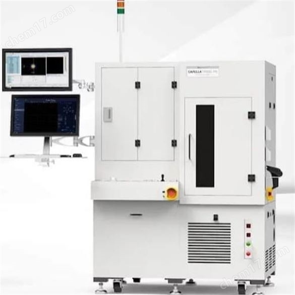
Low pressure chemical vapor deposition system LPCVD
NegotiableUpdate on 05/07
- Model
- Nature of the Manufacturer
- Producers
- Product Category
- Place of Origin
Overview
Introduction to Low Pressure Chemical Vapor Deposition System LPCVD: $r $n1. Meets the high temperature and rapid cooling requirements for graphene and carbon nanotube research $r $n2. Quartz chamber with a diameter of 200 millimeters $r $n3. The design of the internal quartz tube is easy to disassemble and clean $r $n4. The substrate size can reach a diameter of 150 millimeters $r $n5. Three zone resistance furnace with a uniform temperature zone of 150 millimeters
Product Details
1 Product Overview:
Low pressure chemical vapor deposition system(LPCVD)It is a technology that uses heating to react gaseous compounds on the surface of a substrate under low pressure conditions and deposit them to form a stable solid thin film. This system is used in semiconductor manufacturing, power electronics, optoelectronics, and other fieldsMEMSSuch fields have wide applications.LPCVDThe system can form a uniform thin film on the substrate surface by precisely controlling parameters such as temperature, pressure, and gas flow rate, meeting various process requirements.
2 Equipment usage:
LPCVDThe main purposes of the system include:
Thin film deposition: used for depositing various thin film materials, such asPoly-Si(Polycrystalline silicon)Si3N4(Silicon nitride)SiO2(Silicon dioxide), phosphosilicate glass, borophosphosilicate glass, amorphous silicon, and refractory metal silicides. These thin films are used in semiconductor devices, power electronic devices, optoelectronic devices, and moreMEMSPlays a crucial role in the structure.
Semiconductor manufacturing: In the process of manufacturing semiconductor integrated circuits,LPCVDThe system is used to form key structures such as gate oxide, surface passivation layer, nitride stress buffer layer, sacrificial oxide layer, and barrier oxide layer.
Optoelectronic applications: In the field of optoelectronics,LPCVDThe system is used to prepare optical thin films such as optical waveguides, variable refractive index layers, and anti reflection layers to enhance device performance.
3 Features of the equipment
LPCVDThe system has the following characteristics:
Low pressure environment: Deposition under low pressure conditions helps reduce collisions and scattering of gas molecules, improving the uniformity and quality of thin films.
High precision control: The system adopts advanced temperature, pressure, and gas flow control technology, which can accurately control various parameters during the deposition process, ensuring the accuracy and consistency of the film.
Multipurpose: capable of depositing various thin film materials to meet different process requirements, with wide applicability.
Efficiency: Due to low working pressure, the average free path and diffusion coefficient of gas molecules are large, and dense packing can be used to improve productivity.
4 Technical parameters and features:
1. Meet the high temperature and rapid cooling requirements for graphene and carbon nanotube research
2. diameter200Millimeter quartz chamber
3. The design of the internal quartz tube is easy to disassemble and clean
4. The substrate size can reach the diameter150millimeter
5. Three zone resistance furnace,150Millimeter uniform temperature range
6. High temperature can reach1000°C
7. Use throttling typeVATDownstream pressure control of butterfly valve50 mTorrto500 mTorrbetween
8. 8cubic foot/Divided byEbara ESA25-DDry vacuum pump-Two dry vacuum
Similar Product Recommend