-
E-mail
wangxing@yzqjm.com
-
Phone
15316162949
-
Address
No. 666 Zhenhua Road, Xihu District, Hangzhou City, Zhejiang Province
Product Categories
Hangzhou Yuzhiquan Precision Instrument Co., Ltd
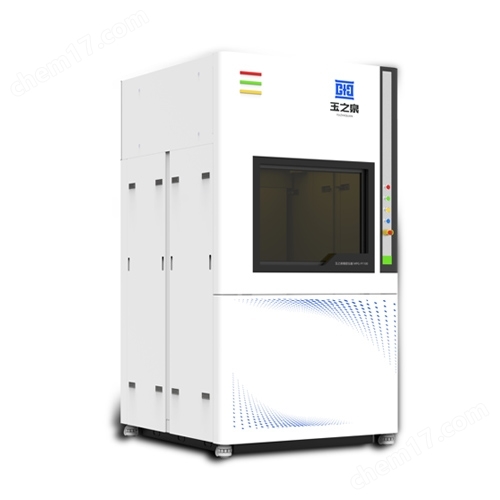
Large area 2.5D structural processing
NegotiableUpdate on 02/10
- Model
- Nature of the Manufacturer
- Producers
- Product Category
- Place of Origin
Overview
Large area 2.5D structure processing technology refers to precise processing on large-sized substrates to form a wide range of 2.5D structures. This technology combines high-precision microfabrication processes and automation equipment, enabling highly consistent structural processing over large areas, and is widely used in fields such as integrated circuits, optical devices, sensor arrays, etc.
Product Details
Overview of Large Area 2.5D Structural Processing
1.1 Definition of 2.5D Structure
The 2.5D structure is a design approach that falls between 2D (two-dimensional) and 3D (three-dimensional) structures. It refers to the formation of a composite structure with both planar layout and certain three-dimensional features by processing a certain degree of vertical structure or local depth structure on a two-dimensional substrate. This structure is commonly used in fields such as integrated circuits, sensors, microfluidic systems, and optoelectronic components.
In traditional two-dimensional (2D) manufacturing, all structures are limited to a plane and cannot effectively achieve space utilization and complex design; In three-dimensional (3D) manufacturing, the difficulty and cost of design and processing are relatively high. The 2.5D structure creates a certain three-dimensional effect by increasing the height difference on a two-dimensional plane, while maintaining relative simplicity and cost-effectiveness in manufacturing.
1.2 Large area 2.5D structural processing technology
Large area 2.5D structure processing technology refers to precise processing on large-sized substrates to form a wide range of 2.5D structures. This technology combines high-precision microfabrication processes and automation equipment, enabling highly consistent structural processing over large areas, and is widely used in fields such as integrated circuits, optical devices, sensor arrays, etc.
The core of this technology lies in the ability to process local depth and vertical structures on large-sized substrates, while ensuring processing accuracy and consistency. This requires high-precision equipment such as lithography machines, laser engraving machines, nanoimprint machines, etc. to meet the needs of different materials and applications.


2. Technical advantages
2.1 High precision and high consistency
One of the core advantages of 2.5D structural processing is its high precision and high consistency. Through advanced photolithography, laser engraving and other technologies, micro - or even nano level processing accuracy can be achieved on large-sized substrates. Accurate control during the processing ensures the consistency and reliability of the product, especially in the manufacturing of electronic and optical components.
2.2 Improve design flexibility
2.5D structural processing technology can integrate components with different functions, such as sensors, conductive paths, and optical components, on the same substrate. This design flexibility enables products to have greater potential in functional integration, system optimization, and other aspects, meeting the modern industrial demand for high integration and multifunctionality.
2.3 Adapt to multiple materials
Support the processing of various materials, including silicon, glass, plastic, metal, etc. Due to the different optical, electronic, and thermal properties of different materials, 2.5D structural processing can select suitable materials for processing according to needs, providing customized solutions for various industries.
2.4 Cost effectiveness
Compared with traditional 3D structural processing techniques, 2.5D processing has significant advantages in processing difficulty and cost. Due to the fact that the processing is mainly concentrated on a two-dimensional plane and only deep processing is carried out in specific areas, it avoids the complexity and high cost of manufacturing a complete three-dimensional structure, and has higher cost-effectiveness.
2.5 Improve functional integration
By processing multi-layer structures on the substrate, high integration of different functions can be achieved. For example, optical and electronic components can be precisely docked on the same substrate, improving product integration and functionality. The application of this technology not only improves product performance, but also achieves better optimization in size and weight.
3. Application Fields
3.1 Microelectronics and Semiconductors
In the microelectronics and semiconductor industries, large-area 2.5D structural processing technology is widely used in the manufacturing of integrated circuits (ICs) and system in package (SiP). Through 2.5D technology, multiple functional modules can be integrated on large-sized substrates, improving integration, reducing signal interference between components, and lowering power consumption.
For example, in the manufacturing process of high-performance processors, 2.5D structure processing can interconnect circuits at different levels, thereby improving the computing power and bandwidth of the chip and meeting the needs of modern data processing.
3.2 Optics and Optoelectronics
In the fields of optics and optoelectronics, 2.5D processing technology can manufacture high-precision optical devices such as fiber couplers, optical diffraction gratings, optical waveguides, etc. By processing tiny optical structures on the substrate, precise manipulation and transmission of optical signals can be achieved.
In addition, products such as photoelectric sensor arrays, lasers, and display panels often use 2.5D structural processing technology to meet higher precision requirements and performance standards.
3.3 Biomedical and Medical Devices
In the fields of biomedical and medical devices, 2.5D structural processing technology is used to manufacture devices such as cell scaffolds and microfluidic chips. By manufacturing tiny three-dimensional structures on substrates, support and guidance for cell growth can be achieved, promoting the development of biomedical materials.
3.4 Sensors and MEMS
In the field of sensors and microelectromechanical systems (MEMS), 2.5D structural processing technology is used to manufacture precision devices such as microsensors, accelerometers, gyroscopes, etc. By fabricating microstructures of different depths and shapes on substrates, high-precision sensing and detection functions can be achieved, which are widely used in industries such as automotive, aviation, and consumer electronics.
3.5 Solar Energy and Energy
In the solar and energy industries, large-scale 2.5D structural processing technology is used to manufacture solar cells and energy conversion components. By fabricating microstructures on optoelectronic components, the absorption efficiency of light and the conversion efficiency of electrical energy can be improved, promoting the advancement of renewable energy technology.

