-
E-mail
wei.zhu@shuyunsh.com
-
Phone
17621138977
-
Address
Room 602, Building 3, G60 Science and Technology Innovation Cloud Corridor, Lane 288, Qianfan Road, Songjiang District, Shanghai
Product Categories
Shuyun Instrument (Shanghai) Co., Ltd


Hard X-ray photoelectron spectrometer HAXPES
NegotiableUpdate on 01/09
- Model
- Nature of the Manufacturer
- Producers
- Product Category
- Place of Origin
Overview
Hard X-ray photoelectron spectroscopy (HAXPES) is used for the next-generation transparent luminescent materials, which utilize nano quantum dots (QDs) with diameters ranging from 10nm to 50nm. By combining XPS (Al Ka X-ray) and HAXPES (Cr Ka X-ray) to analyze the same microscopic characteristic region, detailed deep structural analysis of QDs can be conducted.
Product Details
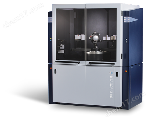
PHIGENESIS Model 900 for HAXPES
Exploration of Depth Without Sputtering Etching
The next generation of transparent luminescent materials uses nano quantum dots (QDs) with a diameter of about 10nm~50nm, combined with XPS (Al Ka X-ray) and HAXPES (Cr Ka X-ray) to analyze the same microscopic characteristic region, allowing for detailed deep structural analysis of QDs.
The combination of XPS and HAXPES can be used for depth resolution, quantitative analysis, and chemical state analysis of nanoparticles, thereby avoiding damage caused by ion beam sputtering.

hardX-ray photoelectron spectrometer HAXPESAnalysis of Deep Interface
Among the two X-ray sources, only Cr Ka XPs can detect Y0, with the Cr layer located 14nm below the surface. The fitted spectrum determined the chemical state of Cr. In addition, by comparing the Cr Ka spectra with photoelectron take-off angles of 90 ° and 30 °, it was found that the intensity of the oxide was higher at shallower take-off angles (with higher surface sensitivity), indicating that the Cr oxide was at the interface between the Y, 0, and Cr layers.

PHI hard X-ray photoelectron spectrometerDetection of Core Electronics
Cr Ka provides additional core electrons that cannot be obtained by Al Ka based high-energy photoelectrons, typically with multiple additional transitions available for analysis.

Application field
Mainly used in solid materials and device fields such as batteries, semiconductors, photovoltaics, new energy, organic devices, nanoparticles, catalysts, metal materials, polymers, ceramics, etc.
Advanced functional materials used in all solid state batteries, semiconductors, photovoltaics, catalysts, and other fields are complex multi-component materials, and their development relies on continuous optimization of chemical structure and performance. The new surface analysis instrument "PHI GENESIS" provided by ULVAC-PHI, Inc. is a fully automatic multifunctional scanning focused X-ray photoelectron spectrometer with * performance, high automation, and flexible scalability, which can meet all analysis needs of customers.
Application of PHI GENESIS Multi functional Analysis Platform in Various Research Fields
Battery AES/Transfer Vessel
PA-AES Li chemical imaging of LiPON/LiCoO 2 cross-section
Li based materials such as LiPON are sensitive to electron beam irradiation.
The high sensitivity energy analyzer provided by PHI GENESIS can quickly obtain AES chemical imaging at low beam current (300pA).

Organic devices UPS/LEIPS/GCIB
Measurement of band structure using UPS/LEIPS and Ar GCIB
(1) Surface of C60 film
(2) After cleaning the surface of C60 film
(3) C60 film/Au interface
(4) Au surface
The energy level structure of the organic layer can be determined through UPS/LEIPS analysis and Ar GCIB deep analysis.

Semiconductor XPS/HAXPES
Semiconductor devices are typically composed of complex thin films containing many elements, and their development often requires non-destructive analysis of the chemical states at the interfaces. It is necessary to use HAXPES to obtain information from deep interfaces, such as GaN under gate oxide films.

Microelectronics HAXPES
The HAXPES analysis data shows that the content of metallic Sn is higher than that of XPS analysis data due to the oxidation of the Sn ball surface. As the depth increases, the content of metallic Sn increases, which is in line with the characteristic of HAXPES analysis depth being deeper than XPS analysis depth.