- Phone
-
Address
Room 2802, Building T4, Yinxuan Center Building, Bao'an District, Shenzhen
Product Categories
Wechsler Nanosystems GmbH, Germany
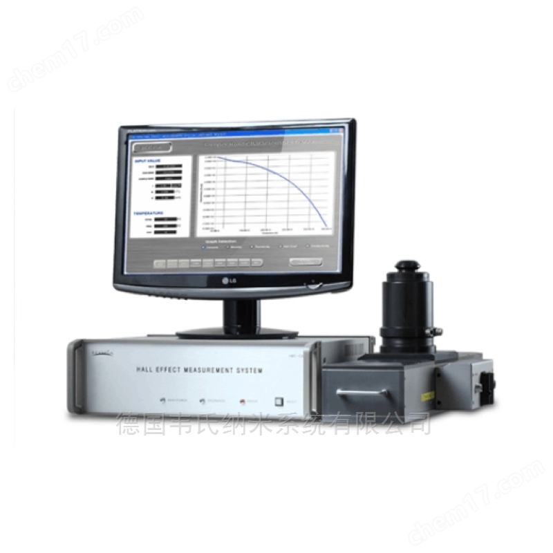
HMS-7000 Hall Effect Tester
NegotiableUpdate on 06/26
- Model
- Nature of the Manufacturer
- Producers
- Product Category
- Place of Origin
Overview
The HMS-7000 Hall Effect Tester is used to measure key electrical parameters of semiconductor materials, such as carrier concentration and mobility. ECOPIA's HMS series Hall effect measurement system is renowned for its high precision, compact design, and easy operation. It features a constant current source, van der Waals law converter, low-temperature measurement system, and magnetic field strength input system. This system can measure various electrical characteristics, support analysis of multiple semiconductor materials, and is widely used in major research institutions and universities.
Product Details
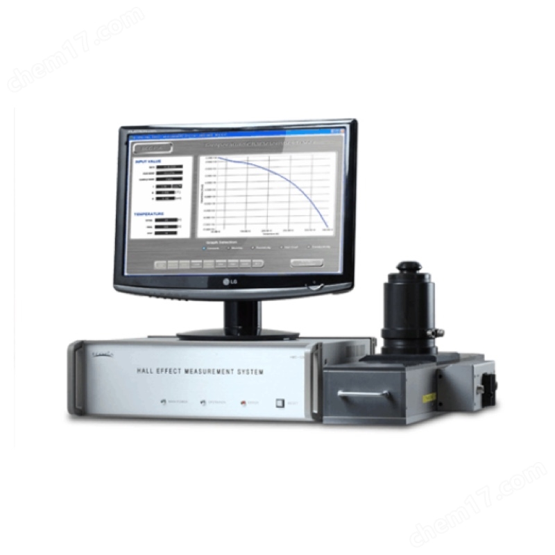

The Hall effect tester is mainly used to measure important parameters such as carrier concentration, mobility, resistivity, Hall coefficient, and conductivity type of semiconductor materials. These parameters must be controlled in advance to understand the electrical properties of semiconductor materials. Therefore, the Hall effect tester is a tool for understanding and studying the electrical properties of semiconductor devices and semiconductor materials.
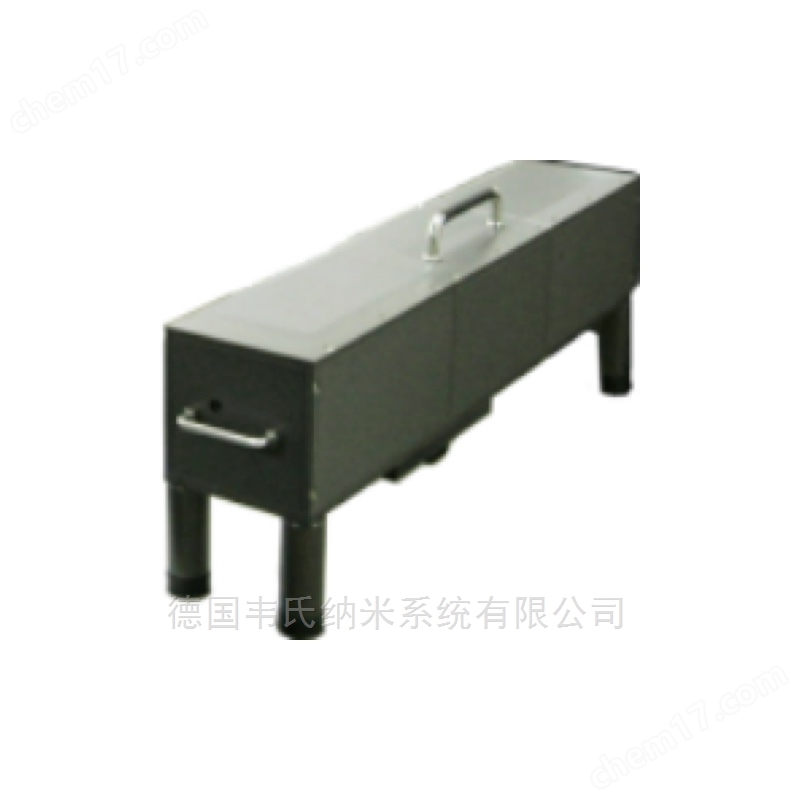
The HMS series Hall effect measurement system of ECOPIA company mainly consists of a constant current source, a van der Waals law terminal converter, a low-temperature (77K) measurement system, and a magnetic field intensity input system. It has all the components and configurations for studying the Hall effect of semiconductor materials and is a very mature instrument system. At the same time, HMS series instruments have obtained multiple Hall effect measurement systems and methods, representing the * quality and reasonable product prices of Hall effect measurement, and have been recognized by * customers. This product passed CE certification in July 2004.
Product Features:
1. Reliable accuracy and reproducibility
The constant current source (1nA~20mA) adopts a six level current range setting to reduce the error that can be received; The van der Waals rule conversion effectively reduces instrument noise using non-contact devices; Targeted design of software and hardware ensures that each experimental data is the average of multiple tests, resulting in excellent data reproducibility of the instrument.
2. Product miniaturization and simplified operation
The small-sized magnetic field strength input system uses permanent magnets and liquid nitrogen low-temperature measurement system (77K) to ensure that the instrument operation is very simple; Two different sizes of traditional sample plates (20 * 20mm, 6 * 6mm) and a sample plate with spring clips (SPCB) make it easier to measure thin film samples of different sizes and materials. The spring clip sample plate, which is different from the traditional sample plate, makes the production of Hall electrodes more convenient and causes less damage to the sample.
3. I-V curve and I-R curve measurement
Using charts, measure the current voltage and current resistance relationships between the four points (A, B, C, D) of the probe, and use this to evaluate the quality of the sample's ohmic contact and understand its basic electrical characteristics.
4. Diverse experimental results
The experimental results are automatically calculated by software, which can simultaneously obtain bulk carrier concentration, sheet carrier concentration, mobility, resistivity, Hall Coefficient, magnetoresistance, vertical/horizontal ratio of resistance, and so on.

Product composition:
Host (precision constant current source+Vanderburg rule terminal converter)/magnet package (including sample board)/software, etc.
Product Specifications
1. Main instrument parameters
Input current: 1nA~20mA;
Electrical resistivity: 10exp (-5)~10exp 7 Ω· cm;
Carrier concentration: 10exp7~10exp21 cm-3;
Migration rate: 1~10exp7 cm2/Volt. sec;
Magnetic field strength: 0.37T, 0.55T, 1T, 0.25~1T variable field magnet;
Sample measurement board: PCB sample board, SPCB spring sample board, wafer sample board, etc;
Sample size: 5mm x 5mm~20mm x 20mm (optional 30mm or 2-inch sample board);
Measurement temperature: room temperature, 77K liquid nitrogen bath;
2. Software operating environment
Under XP/Win7/Win8/Win10 environments

3. Experimental results
Body carrier concentration, surface carrier concentration;
mobility;
Hall coefficient;
Resistivity, block resistance;
Magnetoresistance;
The aspect ratio of resistance;
4. Instrument size and weight
Host size: 360 x 300 x 105 mm (W x H x D) Magnet Kit size: 200 x 120 x 110 mm (W x H x D);
Net weight: 7.7 kilograms;
5. Measuring materials
All semiconductor thin films (P-type and N-type) including Si, SiGe, SiC, ZnO, GaAs, InGaAs, InP, GaN, ITO, etc;