-
E-mail
1276198359@qq.com
-
Phone
13621795675
-
Address
Room 202, Building B, Zhengjue Technology Building, Lane 1356, Xinyuan Road, Minhang District, Shanghai
Product Categories
- Pharmaceutical industry particle analyzer
- Particle size analyzer
- Surface Cleanliness Tester
- Leak detection test of high-efficiency filter in clean room
- Fully automatic particle counter
- Liquid particle analyzer
- Oil spectrum analyzer
- Chip manufacturing testing equipment
- Zeiss Electron Microscope Products
- Optical 3D scanning equipment
- Bridge type coordinate measuring machine
Shanghai Hansen Scientific Instrument Co., Ltd

Zeiss Sigma series products
NegotiableUpdate on 01/01
- Model
- Nature of the Manufacturer
- Producers
- Product Category
- Place of Origin
Overview
The Zeiss Sigma series products closely integrate field emission scanning electron microscopy (FE-SEM) technology with excellent user experience. By utilizing Sigma's intuitive workflow, imaging and analysis programs can be easily implemented, improving work efficiency. You can collect more data in a shorter amount of time.
Product Details
Zeiss Sigma series productsClosely integrate field emission scanning electron microscopy (FE-SEM) technology with a good user experience. By utilizing Sigma's intuitive workflow, imaging and analysis programs can be easily implemented, improving work efficiency. You can collect more data in a shorter amount of time. Striving for excellence in high-resolution imaging - using low voltage to achieve better resolution and contrast at 1kV or lower voltage. By selecting different detectors, Sigma is widely applicable to your applications: whether it is developing new materials, particles for quality inspection, or biological or geological specimens, this electron microscope can help you study various samples. Under extreme conditions, using variable pressure (VP) imaging and NanoVPlite, excellent images and analysis results can be obtained on non-conductive surfaces even at low voltages.
Zeiss Sigma series productsBringing you a reliable and high-quality nano analysis experience. Sigma360 is an intuitive field emission scanning electron microscope (FE-SEM), an analytical testing platform that can be used for imaging and analysis. Excellent EDS geometry design, providing high-throughput analysis and enabling automatic in-situ experiments.
No matter what type of sample, you can always obtain accurate and reproducible analysis results. Obtain richer image information from sensitive samples at low voltage.

Today's scanning electron microscopy applications require high-resolution imaging at low landing energy (referred to as low voltage or low acceleration voltage) as a standard, as this is crucial for studying samples that are sensitive or non-conductive to electron beams. This allows you to obtain authentic surface information of the sample without interference from deeper background signals of the sample. Gemini's electron gun and detection system have been optimized to achieve high-resolution imaging under low and ultra-low voltage conditions, while enhancing contrast. In a scanning electron microscope, a low acceleration voltage incident electron beam is used to image electron beam sensitive samples due to the limited energy transferred to the sample. Meanwhile, low-energy electron beams have poor penetration through the sample. In this way, you can capture artifact free surface details on sensitive samples with high resolution.
Optimize low acceleration voltage imaging
Electron optical distortion can lead to resolution loss, which is more common in low-voltage images. According to the design, the electron beam thruster technology of Gemini 1 tube is capable of providing excellent low acceleration voltage image resolution. The optimized aperture and high-resolution electron gun mode can now further optimize the imaging effect with low acceleration voltage.
High resolution electron gun mode
In high-resolution electron gun mode, the color difference of the electron beam is reduced, resulting in smaller beam spots. At voltages of 1 kV and below, this mode can provide additional image resolution. The spotlight is set by default to excellent imaging conditions (with optimized electron beam convergence). You can choose to provide a range of optimized apertures for current while ensuring high resolution. An additional spotlight mode can be used to optimize the depth of field of the image.
detector
Usually, high-resolution imaging of sensitive materials can be achieved using low incident electron beam voltage and low electron beam probe beam current. When it comes to detecting electrons excited from the sample, efficient Inlens SE detectors can not only provide high resolution, but also enhance contrast when the probe beam current is less than 10 pA. With the support of intelligent scanning programs (such as drift correction frame averaging), stable processing of samples can be ensured even at high resolutions.
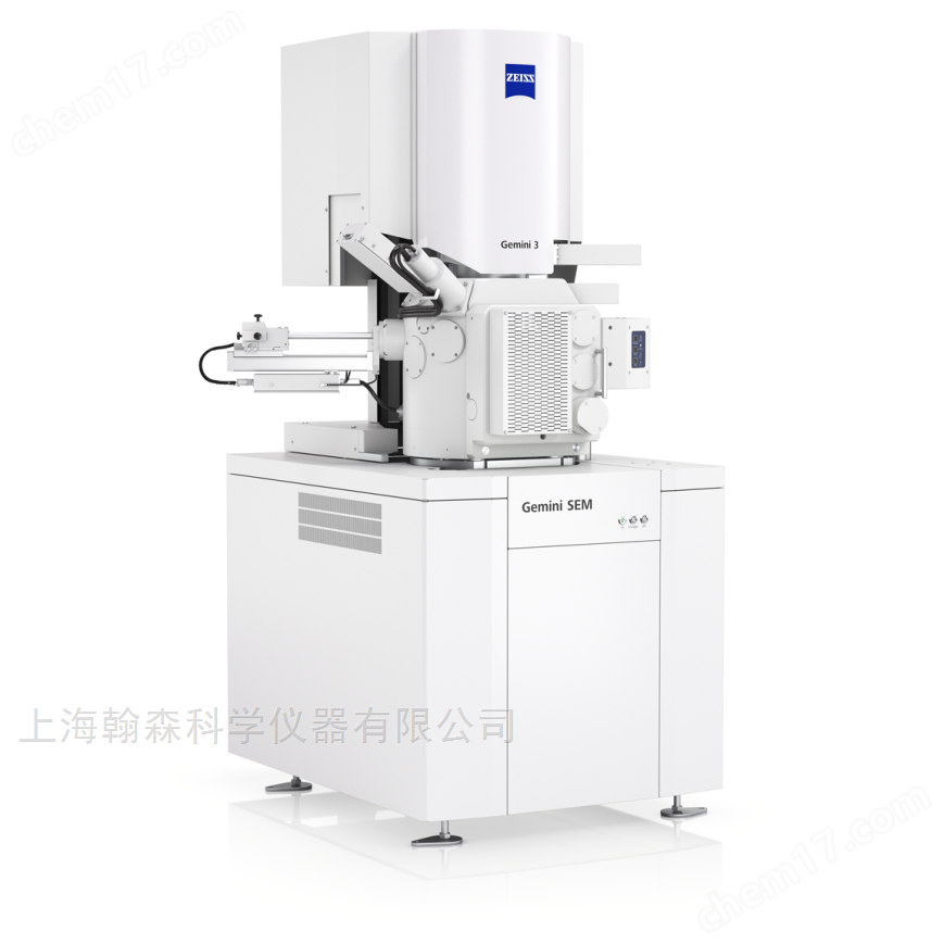
High field emission scanning electron microscope
The excellent sample flexibility of ZEISS GeminiSEM utilizes field emission scanning electron microscopy to explore the unknown, meeting the high requirements for sub nanometer imaging, analysis, and sample flexibility. This system can achieve high-throughput analysis while providing excellent resolution under low voltage, high speed, and high probe current conditions. High image quality and multifunctional advanced imaging mode for efficient detection, excellent analysis. The Zeiss Gemini technology detector, which has been perfected for more than 25 years, has a wide variety of detectors and covers a wide range.
This system can achieve high-throughput analysis while providing excellent resolution under low voltage, high speed, and high probe current conditions. Its observation field is wide, and the cavity is extremely spacious, making it easy to detect even large samples.
The ZEISS GeminiSEM features two opposing EDS ports and a coplanar EDS/EBSD configuration, providing efficient chemical composition and crystal orientation characterization. You can trust high-speed shadowless mapping.
Customize and automate workflow: If you need to test the technical limits of materials, Zeiss can provide you with an automatic in-situ heating and mechanical stress laboratory.
Overview of Application Fields
Failure analysis of mechanical, optical, and electronic components
Fracture analysis and metallographic analysis
Surface, microstructure, and device characterization
Composition and phase distribution
Determination of impurities and inclusions

Similar Product Recommend


