-
E-mail
sales@opton.com.cn
-
Phone
13126536208
-
Address
Oubotong Group, Building 2, No. 1100 Huihe South Street, Chaoyang District, Beijing
Product Categories
Beijing Obotong Optical Technology Co., Ltd

Ultra high resolution field emission scanning electron microscope
NegotiableUpdate on 01/18
- Model
- Nature of the Manufacturer
- Producers
- Product Category
- Place of Origin
Overview
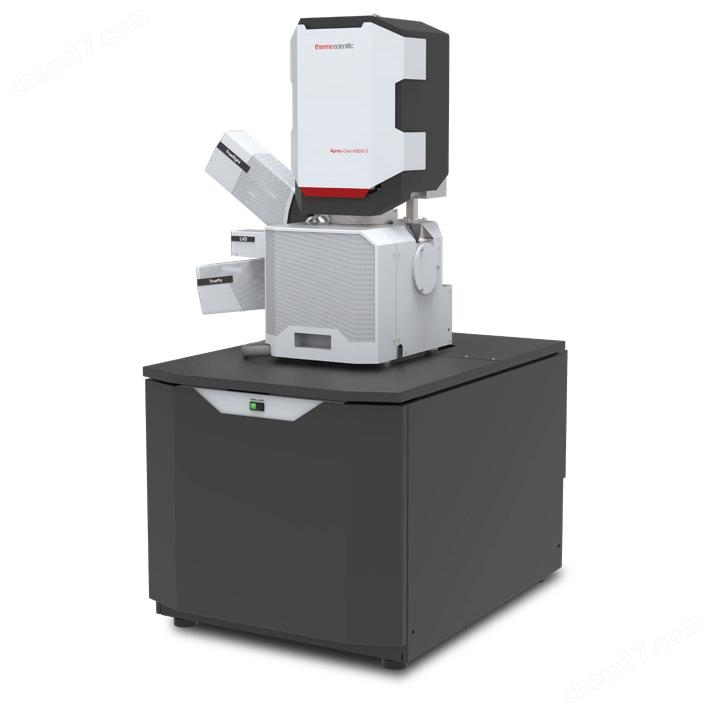
The Thermo Scientific Apreo 2 SEM ultra-high resolution field emission scanning electron microscope is equipped with real-time elemental imaging capabilities and advanced automatic optical systems to achieve gray area resolution, allowing you to no longer worry about microscope performance and focus more on research itself.
Product Details
Thermo Scientific Apreo 2 SEMUltra high resolution field emission scanning electron microscopeEquipped with real-time elemental imaging function and advanced automatic optical system, gray area resolution is achieved, allowing you to no longer worry about microscope performance and focus more on research itself.
The Thermo Scientific Apreo 2 SEM has multifunctionality and high-quality imaging performance. It adopts an innovative final lens design and introduces an electrostatic final lens, supporting high-resolution detection inside the tube. Even for magnetic samples, it can achieve excellent imaging and analysis performance. The all-new Apreo 2 SEM has further optimized its ultra-high resolution imaging capability on the basis of its original performance, and added many new features to enhance its usability. Apreo 2 SEM introduces SmartAlign technology on a durable SEM platform, eliminating the need for manual adjustment by users. Additionally, FLASH automatically performs fine adjustment work, allowing for necessary lens centering, astigmatism correction, and focus correction with just a few mouse movements. In addition, Apreo 2 SEM has a resolution of 1nm at a working distance of 10mm, and a longer working distance no longer means low resolution imaging. The system can also upgrade its real-time element spectrum/image imaging function. For decades, the inherent element analysis process of traditional SEM-EDS has increased the efficiency of element analysis by more than twice. Apreo 2 SEM, Any user can easily obtain analysis results.
☆ Comprehensive analysis
Comprehensive nanometer and sub nanometer resolution performance, suitable for materials such as nanoparticles, powders, catalysts, nanodevices, and bulk magnetic samples;
☆ Flexibility
Very flexible in handling a wide range of sample types, including insulators, sensitive materials, or magnetic samples, and collecting important data for your application;
SmartAlign technology
Using SmartAlign technology (intelligent adjustment of optical system) to achieve automatic adjustment of optical system and reduce maintenance time;
☆ Advanced automation
Advanced automation includes FLASH technology for automatic image fine-tuning, undo, user guidance, and map imaging stitching;
☆ Real time quantitative EDS
Elemental information is within reach, utilizing ColorSEM technology to provide real-time quantitative analysis of element surface distribution imaging, resulting in faster and more convenient results acquisition;
☆ Standard workflow operations
Built in User Guidance function, whether beginners or experienced, can quickly get started and stably obtain experimental data.
Thermo Scientific Apreo 2 SEMUltra high resolution field emission scanning electron microscopeparameter
Source of emission: High stability Schottky field emission electron gun
Resolution:
| model | Application 2 C | Application 2 S |
| Final lens | static electricity | composite |
| 高真空 | ||
| 15kV | 0.9nm | 0.5nm |
| 1kV | 1.0nm | 0.8nm |
| 500V | 1.2nm | 0.8nm |
Acceleration voltage range: 200V~30kV
Landing voltage range: 200eV~30keV
Probe current range: 1pA -50nA, continuously adjustable (upgradable up to 400nA)
Sample Room: A large storage space with a width of 340mm from left to right. The sample room can accommodate 12 expandable interfaces, including 3 spectrometer interfaces (2 of which are located at 180 ° diagonal positions)
Sample stage: Five axis optimal center fully automatic motor drive X=110 mm, Y=110 mm, Z=65 mm, T=-15 º~90 º, R=360 º (continuous rotation)
Multi purpose SEM sample installation stage, capable of simultaneously placing 18 standard sample holders (with a diameter of 12mm)
Detector system:
Sample Room Secondary Electronic Detector ETD
Backscattered electron detector T1 inside the tube
Secondary electron detector T2 inside the tube
Secondary electronic detector T3 inside the tube (upgradable)
IR-CCD infrared camera in the sample room (observing the height of the sample stage)
Nav Cam color optical camera for image navigation+ ™
Control system:
Operating System: Windows 10
Image display: 24 inch LCD monitor with a display resolution of 1920 × 1200
Support user-defined GUI, capable of displaying 4 images in real-time simultaneously
The software supports undo and redo functions
Similar Product Recommend