-
E-mail
research@resemtech.com
- Phone
-
Address
C305, No. 88 Baifu Road, Kunshan Economic Development Zone, Jiangsu Province
Product Categories
- Energy dispersive spectroscopy (EDS)
- Ion sputtering instrument (gold plating machine, coating instrument)
- UV ozone cleaner (Filgen)
- Oxford energy spectrometer (elemental analyzer)
- Second hand scanning electron microscope, second-hand electron microscope, second-hand SEM EDX, second-hand EDX
- New scanning electron microscope (Hitachi)
- Ion grinder (Hitachi)
Kunshan Ruisai Qi Precision Instrument Co., Ltd
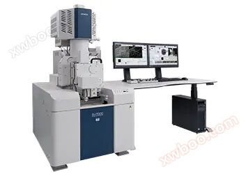
New Schottky field emission scanning electron microscope SU7000
NegotiableUpdate on 12/21
- Model
- Nature of the Manufacturer
- Producers
- Product Category
- Place of Origin
Overview
The new Schottky field emission scanning electron microscope SU7000 can obtain various information of the sample and achieve high-throughput analysis. The SU7000 shortens the time to obtain multiple information of the sample by collecting multiple signals, truly realizing high-throughput analysis
Product Details
New Schottky field emission scanning electron microscope SU7000
Various information about the sample can be obtained to achieve high-throughput analysis
The Schottky field emission scanning electron microscope SU7000 shortens the time required to obtain various information about the sample by collecting multiple signals, truly achieving high-throughput observation and analysis.
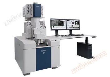
SU7000 appearance diagram
Scanning electron microscopy (SEM) can obtain various information from microstructure to composition by detecting signals such as secondary electrons, backscattered electrons, X-rays, etc. excited by samples. Therefore, it is widely used in many fields such as nanotechnology, semiconductors, electronic devices, biology, materials, etc. With the continuous expansion of the application scope of SEM, there is a further demand for shortening observation time and rapid and efficient signal acquisition.
The SU7000 adopts a newly designed detector, which greatly improves the detection and separation ability of secondary electronic signals and backscattered electronic signals. Previously, we had to adjust the distance between the sample and the lens (working distance/hereinafter referred to as WD) based on the obtained signals to set the most suitable observation and analysis conditions. However, with the newly developed sample chamber and detector system, SU7000 can more efficiently receive various signals without changing WD, shortening the time for sample observation and analysis and improving testing efficiency.
Moreover, the SU7000 is equipped with a 6-channel display interface (previous models could only display 4 channels simultaneously), further upgrading the SEM control system and significantly improving the signal acquisition speed, thereby achieving high-throughput observation of samples.
It also comes standard with a large sample compartment and an accessory interface, which can be used for observation and analysis of various samples.
Hitachi High Tech will showcase this SU7000 at the "Microscopy&Microanalysis" event held in Maryland, USA from August 5th (Sunday) to August 9th (Thursday), and at the "JASIS 2018" event held at the Makuhari Exhibition Center (Chiba City, Chiba Prefecture) from September 5th (Wednesday) to September 7th (Friday). It is expected that global sales will reach 150 units annually.
Hitachi High Tech Scientific Systems Division aims to become the world's number one in the electron microscope industry by 2020 as its mid-term strategic goal. In the future, it will continue to fully promote product research and development and market promotion, and strive to make greater contributions to the global manufacturing industry. As an advanced and cutting-edge innovative enterprise, our goal is to become a world-class enterprise that provides high-tech and solutions, always standing in the customer's position and quickly meeting customer and market needs.
【 Main Features 】
Under the same WD conditions, it is possible to simultaneously observe secondary electrons, backscattered electrons, and perform X-ray analysis
2. It can achieve up to 6 channels of detection and display simultaneously
3. Image data can also be obtained at a maximum pixel size of 10240 x 7680
4. Up to 18 accessory interfaces can be configured in devices of the same level
5. Supports low vacuum mode with a minimum pressure of 300Pa (optional)
*Spatial resolution below 1 nm/1 kV
Main specifications
Product Name |
SU7000 |
electronic source |
ZrO/Wwarm-upEmission (Schottky thermal field emission)) |
Secondary electronic resolution |
0.8 nm(Acceleration voltage)15 kV) 0.9 nm(Acceleration voltage)1 kV) |
accelerating voltage |
0.1~30 kV |
magnification |
20~2,000,000times |
beam |
maximum200 nA |
sample stage |
X/Y/Z : 135 x 100 x 40(mm) |
Key Concept
-
Versatile Imaging Capability
The SU7000 excels in fast acquisition of multiple signals to address expansive SEM needs, from imaging a wide field of view to visualizing sub-nanometer structures and everything in between.
The incorporation of newly designed electron optics and detection systems allows for efficient simultaneous acquisition of multiple secondary electron and back-scattered electron signals. -
Multi-Channel Imaging
The number of the detectors mounted on the SEM is ever increasing, along with the need to display all collected information effectively.
The SU7000 is capable of processing, displaying, and saving up to 6 signals simultaneously to maximize information acquisition. -
Wide Variety of Observation Techniques
The specimen chamber and the vacuum system are optimized for:
・ Large specimen size
・ Sample manipulation at various axes
・ Variable pressure conditions
・ Cryogenic conditions
・ Heating and cooling in-situ observation -
Microanalysis
The electron gun is equipped with a Schottky emitter that provides up to 200 nA beam current to accommodate various microanalysis applications.
The specimen chamber and port layout are designed to incorporate multiple analytical options including EDX, WDX, EBSD, cathodoluminescence, and more.
The SU7000 with the combination of numerous analytical accessories unifies multi-discipline techniques in a single platform.
Imaging Performance
Enhanced Information Acquisition
The advanced detection system of the SU7000 streamlines acquisition of structural, topographical, compositional, crystallographic, and other types of information by minimizing changes to microscope conditions, such as working distance or accelerating voltage.
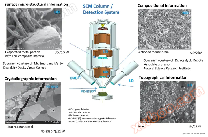
Single-Scan Multi-Signal Imaging
Specimen: Organic-coated gold rods
Specimen courtesy of: Mr. Smart and Ms. Je Chemistry Dept.,
Vassar College
Specimen: Organic-coated gold rods
Specimen courtesy of: Mr. Smart and Ms. Je Chemistry Dept.,
Vassar College
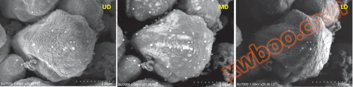
Simultaneous image acquisition for surface micro-structural information (UD), surface coating (MD), and overall topographic information (LD). Acceleration voltage: 1 kV
Intuitive Graphical User Interface
Enhanced Signal Display
- Customizable display modes.
- Single and Dual-monitor configurations.
- Simultaneous image display up to 4-ch (single) and 6-ch (dual).
- Chamber Scope and SEM MAP for optical stage navigation.
Highly Flexible Screen Layout
The software is capable of display 1, 2, or 4 signals including the chamber scope or SEM MAP on a single monitor.
Additionally, the operation panel can be customized to display submenus anywhere on the screen.

Dual Monitor
The first monitor can be used as a dedicated image display while the second monitor is utilized for operation.
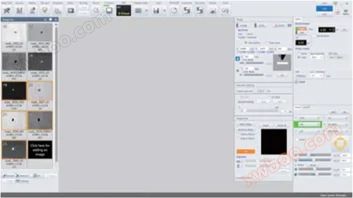
Five detector images (UD, LD, UVD, MD, and PD-BSED) and SEM MAP of non-metallic inclusions in a steel specimen are displayed (left).
The screen shows the operation panel menu and the thumbnail image window on one screen (right).
The dual-monitor configuration supports increased productivity with expanded w

Expandable Observation and Analysis
Large specimen chamber and large stage
The specimen chamber can accommodate a tall specimen of φ 200 mm or 80 mm in height and 18 accessory ports. The large stage travels 135 mm (X) x 100 mm (Y) and can accept up to 2 kg of specimen.(*)Large specimen or variable type of sub-stages can be easily mounted on the front-opening large stage door.
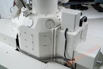
external view of the specimen chamber featuring 18 accessories por
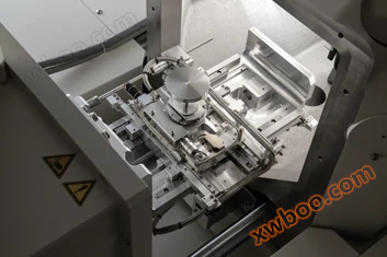
external view of the stage. XY movable range: 135×100 mm
- (*)at 0° tilt
Camera Navigation(*)
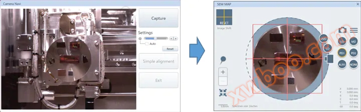
Left: Picture of the sample captured by the camera equipped inside the chamber.
Right: Camera image transferred to the SEM MAP screen for navigation.
The camera navigation feature correlates an optical image to the target observation area.
The camera installed in the specimen chamber captures the specimen image at the time of specimen introduction. The image is transferred to the SEM MAP screen for a graphically driven navigation interface.
Camera navigation supports a maximum of φ 100 mm specimen.
- (*)
- Camera navigation function is optional
Detection System Enabling Dynamic Observation
The SU7000 supports observation under various environmental conditions. A variety of detectors(*)such as UVD and MD are selectable in addition to the PD-BSED for observation under low-vacuum conditions.
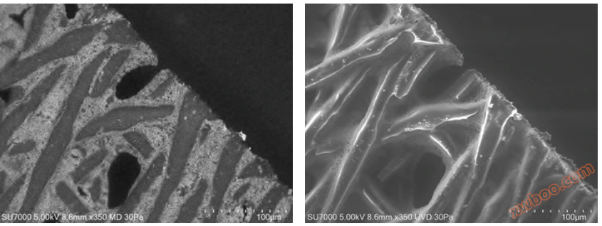
Detector Selection Under Low-Vacuum Conditions
Specimen: Fiber with metallic oxide
Left: MD (Backscattered electron) image
Right: UVD (SE image)
The oxide dispersion and fiber layering state are observed respectively.
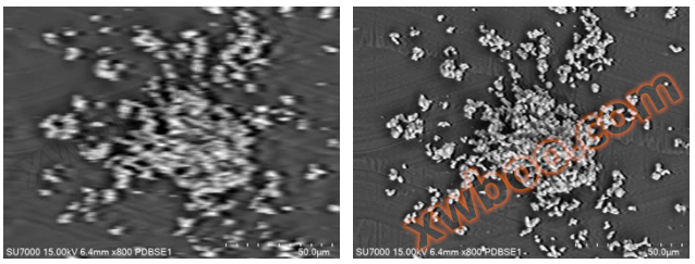
Improved PD-BSED Response Speed
Left: Traditional PD-BSED response at the scan rate of 30 ms x 64 frames
Right: SU7000 PD-BSED image demonstrating improved response and image quality to expand in-situ observation capability
Specifications
| Image Resolution | Resolution SE | 0.8 nm@15 kV | |
|---|---|---|---|
| 0.9 nm@1 kV | |||
| Magnification | 20~2,000,000 x | ||
| Electron Optics | Emitter | ZrO/W Schottky Emitter | |
| Accelerating Voltage | 0.1~30 kV (0.01 kV step) | ||
| Probe Current | Max. 200 nA | ||
| Detectors | Standard Detectors | UD(Upper Detector) | |
| MD(Middle Detector) | |||
| LD(Lower Detector) | |||
| Optional Detectors | PD-BSED(Semiconductor type) | ||
| UVD (Ultra Variable Pressure Detector) | |||
| Variable Pressure(VP) Mode (Option) | Pressure Range | 5~300 Pa | |
| Available Detectors in VP mode | PD-BSED, UVD, UD, MD,LD | ||
| Specimen Stage | Stage Control | 5-axis Motor Drive | |
| Movable Range | X | 0~135 mm | |
| Y | 0~100 mm | ||
| Z | 1.5~40 mm | ||
| T | -5~70° | ||
| R | 360° | ||
| Specimen Chamber | Specimen Size | Max. φ200 mm, Max. 80mm Height | |
| Monitor(Option) | 23 inch LCD(1,920×1,080) , supports dual monitors operation | ||
| Image Display Mode | Large Screen Display Mode | 1,280×960 pixels | |
| Single Image Display Mode | 800×600 pixels | ||
| Dual Image Display Mode | 800×600 pixels、1,280×960 pixels with dual monitors | ||
| Quad Image Display Mode | 640×480 pixels | ||
| Hex Image Display Mode w/dual monitors | 640×480 pixels with dual monitors | ||
| Image Data Saving | Pixel Size | 640 × 480, 1280 × 960, 2560 × 1920, 5120 × 3840, 10240 × 7680 | |
| Optional Accessories | Energy Dispersive X-ray Spectrometer (EDX) | ||
| Wavelength Dispersive X-ray Spectrometer (WDX) | |||
| Electron Backscattered Diffraction Detector (EBSD) | |||
| Cathodoluminescence System (CL) | |||
| Cryogenic Transfer System | |||
| Compatible with various types of sub-stages | |||
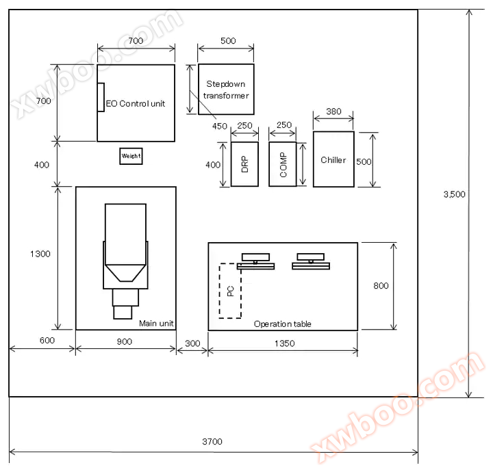
Installation Diagram
Similar Product Recommend


