-
E-mail
317399383@qq.com
-
Phone
15955179814
-
Address
No. 9996 Susong Road, Economic Development Zone, Hefei City, Anhui Province
Product Categories
Hefei Zhongguang Electronic Technology Co., Ltd

Lithography process equipment
NegotiableUpdate on 02/09
- Model
- Nature of the Manufacturer
- Producers
- Product Category
- Place of Origin
Overview
Overview of Lithography Process Equipment Products: $n Applied to 3D Packaging LED、 Main configurations in the fields of microelectromechanical systems, compound semiconductors, power devices, etc.: automatic alignment, automatic exposure, LED light source, machine vision alignment system, high-precision silicon wafer carrier, automatic wedge error compensation system. LED light source: 3 wavelength arbitrary configuration, supporting more application scenarios. High resolution and high uniformity; Long service life and easy maintenance: $n machine vision alignment system: top and bottom dual-mode alignment, large field of view, high precision; Four types of lighting options are available, with strong process adaptability; Free switching between manual and automatic modes
Product Details
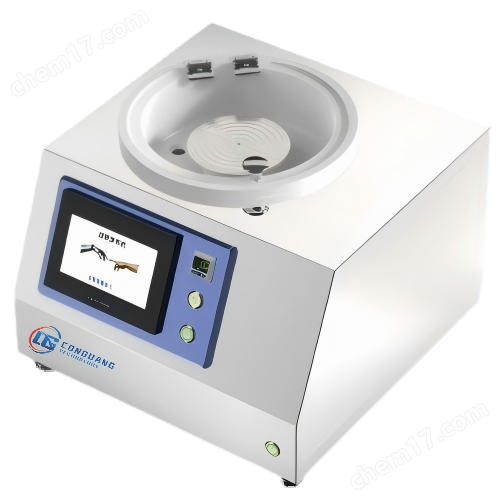
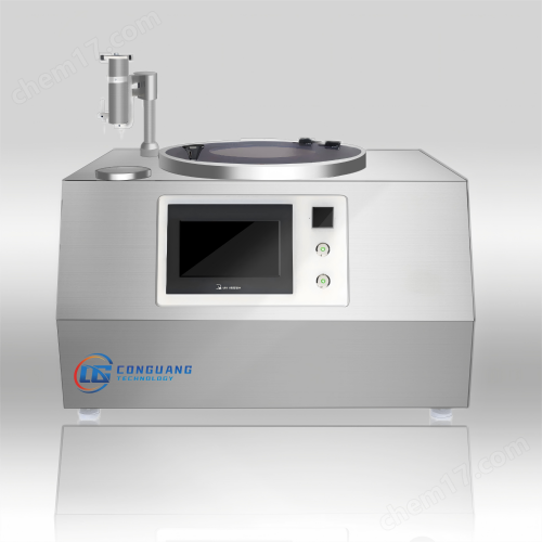
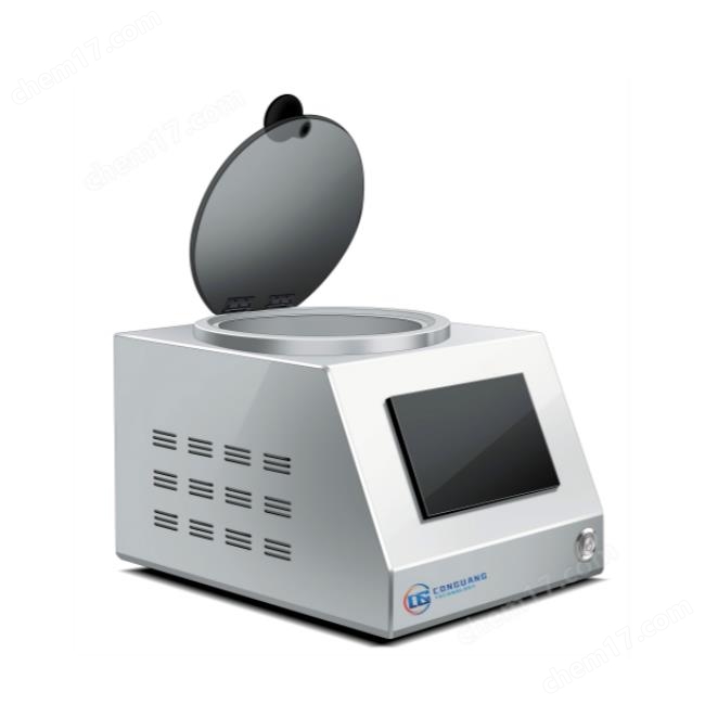
Lithography process equipmentProduct Overview:
Applied to 3D packaging LED、 In the fields of microelectromechanical systems, compound semiconductors, power devices, etc.
Main configuration: automatic alignment, automatic exposure, LED light source, machine vision alignment system, high-precision silicon wafer carrier, automatic wedge error compensation system.
LED light source: 3 wavelengths can be configured arbitrarily, supporting more application scenarios.
High resolution and high uniformity; Long service life and easy maintenance:
Machine vision alignment system: dual-mode alignment at the top and bottom, with a large field of view and high precision; Four types of lighting options are available, with strong process adaptability; Free switching between manual and automatic modes.
Lithography process equipmentTechnical Specifications:
| Mask template, silicon wafer | |
| Silicon wafer size | 8'/ 6' |
| wafer thickness | max.10 mm |
| Mask template size | 9' ×9'/ 7' ×7' (SEMI) |
| Mask thickness | max.6.35 mm |
| exposure mode | |
| contact method | Soft contact, hard contact, vacuum contact |
| Exposure gap | 0~1000 μm |
| Gap accuracy | 1 μm |
| Exposure intensity | 0 ~ ≥40mw/cm 2 |
| Exposure lens | |
| Light source type | LED |
| Exposure wavelength | 365nm,405nm, |
| Uniformity of light intensity | ≤4% 8' / ≤3% 6' |
| resolution | Vacuum contact ≤ 1um |
| Hard contact ≤ 1.5 μ m | |
| Soft contact ≤ 2.2 μ m | |
| Gap ≤ 3.6 μ m | |
| Alignment mode | |
| Top alignment | < ±1 μm |
| Optional bottom alignment | < ±2 μm |
| Top alignment focusing range | 5 mm |
| Bottom alignment focusing range | 5 mm |
| Silicon wafer carrier platform | |
| range of motion | X :± 5 mmy :± 5 mm θ: ± 5 ° |
| resolution | 0.04 μm |
| Top aligned lens | |
| Mobile range | 6' 40~150mm |
| 8' 40~200 mm | |
| Align the bottom with the lens | |
| Mobile range | 6' 40~150mm |
| 8' 40~200 mm | |
| User interface | |
| Windows 10 | Storable process menu |
| Venue service requirements | |
| Vacuum<-0.8 kPa; Nitrogen>0.5 Mpa; Compressed air: 0.6~0.8 Mpa | |
| Power supply demand | |
| Voltage: 230 V ± 10% | Frequency: 50-60 Hz |
| Size and weight | |
| Length x Width x: 1200 x 1000 mm | Height: 1973 mm Weight:~400 kg |