-
E-mail
qeservice@enli.com.tw
-
Phone
18512186724
-
Address
Room 409, Building A, No. 169 Shengxia Road, Pudong New Area, Shanghai
Product Categories
Guangyan Technology Co., Ltd

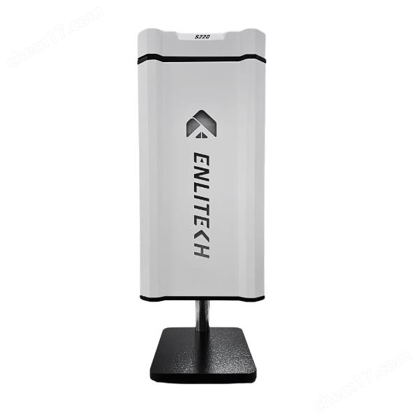
Laser scanning defect spectrometer
NegotiableUpdate on 01/27
- Model
- Nature of the Manufacturer
- Producers
- Product Category
- Place of Origin
Overview
The Laser Scanning Defect Imager is an upgraded version of Laser Beam Induced Current (LBIC) testing. It uses a laser beam with a wavelength energy greater than the semiconductor bandgap to irradiate the semiconductor, generating electron hole pairs. By quickly scanning the surface of the sample, the image distribution revealing internal current changes can be obtained to analyze the distribution of various defects. This helps to analyze the quality of sample preparation and contributes to process improvement.
Product Details
Product Introduction
Master the whole picture within 4 minutes, scan the 100mm x 100mm area with a resolution of 50 microns
excitelightThe Scanning Defect Imager is an upgraded version of Laser Beam Induced Current (LBIC) testing. It uses a laser beam with a wavelength energy greater than the semiconductor bandgap to irradiate the semiconductor, generating electron hole pairs. By rapidly scanning the surface of the sample, the image distribution revealing internal current changes can be obtained to analyze the distribution of various defects. This helps to analyze the quality of sample preparation and contributes to process improvement.
feature
●Scanning the distribution of photocurrent
●Scanning photovoltaic voltage distribution
●Scan the distribution of open circuit voltage and short circuit current
●Analyze surface pollution
●Analyze the distribution of short-circuit areas
●Identify and analyze microcrack areas
●Analyze the distribution of diffusion lengths of a few carriers (function selection)
application

Photovoltaic current distribution of silicon solar cells (405 nanometers)

![]()
6-inch silicon crystal solar cell scan (17 seconds)

Perovskite solar cells

LSD4-OPV photoresponsive current distribution diagram

LSD4-OPV photoresponsive current distribution diagram

Non uniformity analysis with a resolution of 50 µ m

Busbar/grid aspect ratio detection (cross-sectional analysis)


High repeatability (6 repetitions)
Specifications
| project | Parameter description. |
|---|---|
| function | A. Utilizing laser beams with wavelengths higher than the bandgap of semiconductors to generate electron hole pairs, exploring the impact of depletion regions on internal current changes, understanding and analyzing various defect distributions, as a direction for process improvement. b. Capable of scanning the distribution of photocurrent on the surface of the sample. C. Capable of scanning the distribution of photovoltage on the surface of the sample. d. Can scan the distribution of open circuit voltage and short circuit current. e. Capable of analyzing surface pollution. F. Can analyze the distribution of short-circuit areas. G. Capable of identifying and analyzing microcrack areas. H. Ability to analyze the distribution of minority carrier diffusion length (optional). |
| motivation source |
405 ± 10nm laser 520 ± 10nm laser 635 ± 10nm laser 830 ± 10nm laser |
| Scan Area | ≧100mm×100mm |
| laser spot size | Approaching TEM00 mode point |
| Surveying resolution |
A. Scanning resolution ≤ 50 µ m b. The scanning resolution can be set through software |
| Surveying time | <4 minutes (100mm x 100mm, resolution 50um) |
| aspect | 60cm * 60cm * 100cm |
| software | A. LBIC 3D visualization b. 2D cross-sectional analysis (electrode aspect ratio) c. Analysis of photocurrent response distribution (combined with long wavelength laser source) d. Data saving and exporting function |
Similar Product Recommend