-
E-mail
ellen.huang@unicorn-tech.com
- Phone
-
Address
No. 1 Lide International, 1158 Zhangdong Road, Pudong New Area, Shanghai, 609V
Product Categories
Younikon Technology Co., Ltd
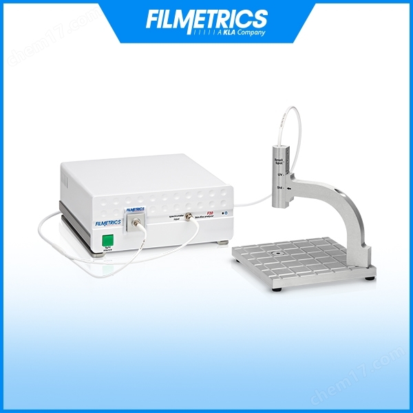


Filmetrics F20 White Light Interference Thickness Gauge
NegotiableUpdate on 01/05
- Model
- Nature of the Manufacturer
- Producers
- Product Category
- Place of Origin
Overview
The Filmetrics F20 white light interference thickness gauge is a high-precision and multifunctional measuring device that can quickly determine the characteristics of film thickness, optical constants, reflectivity, and transmittance. Its non-contact measurement method is suitable for various fragile or sensitive materials, with nanometer level resolution and a wide measurement range (1nm-3mm). This instrument is suitable for various application scenarios, including semiconductor, optical, biomedical and other fields. The F20 film thickness gauge can provide accurate measurement results within seconds, supporting the analysis of single-layer and multi-layer thin films, and providing reliable support for scientific research and industrial production.
Product Details
Filmetrics F20 Single Point Optical Film Thickness Measuring Instrument

Filmetrics F20 White Light Interference Thickness GaugeIntroduction:
Whether you want to know film thickness, optical constants, or material reflectivity and transmittance, the Filmetrics F20 single point optical film thickness gauge can meet your needs. It only takes a few minutes to complete the installation, and the device can obtain measurement results within seconds by connecting to a computer via USB. Based on the characteristics of modular design, the Filmetrics F20 single point optical film thickness measuring instrument is suitable for various applications.
Filmetrics F20 White Light Interference Thickness GaugeFeatures:
Non contact measurement: to avoid damaging the film, suitable for fragile or sensitive materials;
High precision and wide range: vertical resolution up to nanometer level, measurable thickness range from 1nm to 3mm;
Multi scenario applicability: Basically smooth, semi transparent, or low absorption coefficient films can be measured.
Fast measurement speed: After configuration is completed, the measurement can be completed within seconds.
Measurement principle:
When incident light passes through interfaces of different substances, some of the light will be reflected. Due to the fluctuation of light, the reflected light from multiple interfaces interferes with each other, resulting in oscillations in the multi wavelength spectra of the reflected light. From the oscillation frequency of the spectrum, the distance between different interfaces can be determined to obtain the thickness of the material (more oscillations represent greater thickness), as well as other material properties such as refractive index and roughness.

Film layer example:
Thin film characteristics: thickness, reflectivity, transmittance, optical constant, uniformity, etching amount, etc
Film types: transparent and semi transparent films, commonly such as oxides, polymers, and even air
Thin film state: Solid, liquid, and gaseous thin films can all be measured
Thin film structure: single-layer film, multi-layer film; Flat and curved surfaces
Common industrial applications:
Semiconductor film layer |
display technology |
consumer electronics |
Parylene |
photoresist |
OLED |
waterproof coating |
Electronic products/circuit boards |
dielectric layer |
ITO and TCOs |
RFID (Radio Frequency Identification) |
magnetic materials |
gallium arsenide |
Air box thickness |
solar cell |
Medical equipment |
Micro-electromechanical Systems |
PVD and CVD |
Aluminum shell anode film |
silicone rubber |
Product Parameters:
Wavelength range: |
380-1050nm |
light source |
halogen lamp |
Thickness measurement range: |
15nm-70um |
Measurement accuracy: |
0.02nm |
Spot size: |
1.5mm |
Sample table size: |
1mm-300mm |
More parameters can be obtained by contacting us | |||
Measurement diagram:


Similar Product Recommend


