-
E-mail
info@phenom-china.com
-
Phone
18516656178
-
Address
Room T5705, Shanghai Hongqiao Libao Plaza, No. 88 Shenbin Road, Hongqiao Town, Minhang District, Shanghai
Funa Scientific Instruments (Shanghai) Co., Ltd
See you in Wuhan! Funa Technology invites you to attend the 2025 National Conference on Electron Microscopy
Date: 2025-09-23Read: 2
The 2025 National Conference on Electron Microscopy will be held from September 26th to 30th (registration on the 26th, departure on the 30th) at the Wuhan International Convention Center. On the occasion of forging ahead for five autumns and exploring the truth for the benefit of the country, we welcome the 45th anniversary celebration of the establishment of the Chinese Society for Electron Microscopy (International). This year's annual meeting is a special celebration, where microscopicists use their knowledge and dedication to analyze the mysteries of the microscopic world, bravely take on responsibilities for a strong technological country, and constantly strive for progress.
The theme of this year's conference is: Microscopic Pursuit of Dreams for Five Years, Striving to Send Messages to China. This year's annual conference will set up fifteen specialized sub venues according to the disciplines of materials science and life science:
Microscopy theory, instrument methods and techniques;
In situ electron microscopy characterization;
Characterization of microstructure of functional materials;
Structural materials and defects, interfaces, surfaces, phase transitions and diffusion;
The application of advanced microscopic analysis technology in industrial materials;
Scanning probe microscopy characterization (STM/AFM, etc.);
Electron diffraction and electron holography (including SEM, EBSD, and TEM);
The application of focused ion beam (FIB) in materials science;
Low temperature electron microscopy characterization;
Development and application of biomedical electron microscopy technology;
The application of microscopy in the fields of agriculture, forestry, and biological sciences (such as super-resolution microscopy, confocal laser microscopy, etc.);
Research and application of agricultural and forestry electron microscopy;
Advanced material microscopic characterization and cutting-edge innovation;
Microscopic scientific instruments and advanced materials;
Intelligent upgrade and open sharing of microscopy platform.
✦✦✦
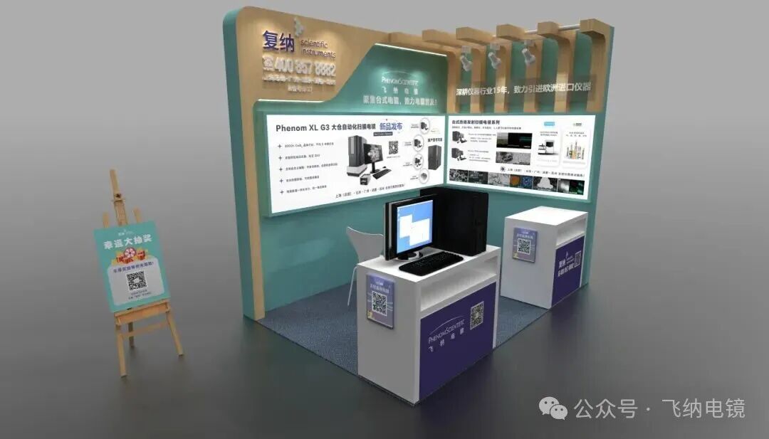
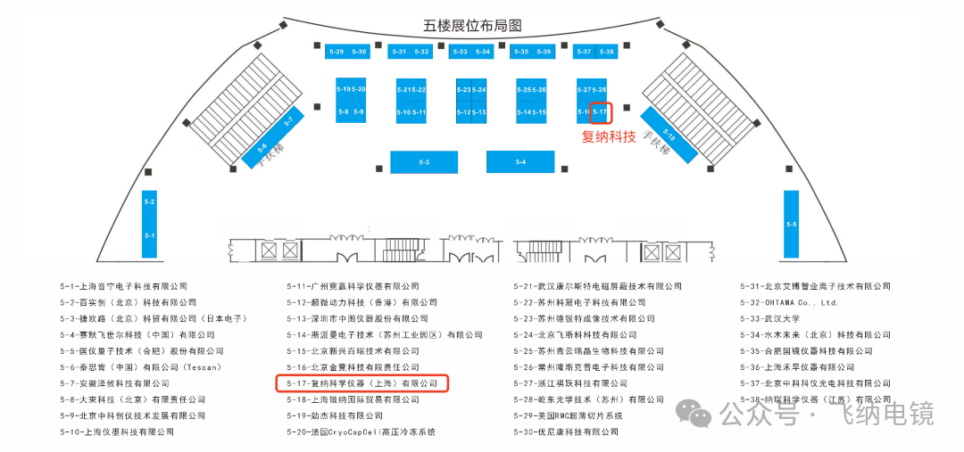
Funa Scientific Instruments (Shanghai) Co., Ltd. (hereinafter referred to as "Funa Technology") has been invited to participate in this conference, and on the occasion of the new product launch, it will exhibit the Phenom XL, an automated scanning electron microscope from Funa Warehouse, on site. Welcome to the 5th floor【5-17】Funa Technology booth testing experience and exchange, jointly exploring the latest material characterization and preparation technologies!
• Meeting time
September 26-29, 2025 (reporting on the 26th)
• Meeting location
Wuhan International Convention and Exhibition Center
Funa Technology booth number5-17
Live interaction
Kapibala, "Garlic Bird" is waiting for you to pick it up
During the conference from September 26th to 29th
Focus on Funa Technology/Feina Electron Microscope official account
Reply 'Chou Award'
Fill out the questionnaire to participate in the interaction!

About Funa Technology
Funa Technology was founded in 2012, focusing on introducing advanced and stable scientific analysis instruments and manufacturing equipment from Europe and America to assist China's scientific research innovation and industrial upgrading. The company has served over 2500 Chinese users and established long-term and stable cooperative relationships with nearly 10 internationally renowned manufacturers, jointly providing high-quality products and professional services to Chinese users. The main business lines are as follows:
Nano microscopy imaging:Phenom desktop scanning electron microscope from the Netherlands, NEOSCAN high-resolution desktop micro CT from Belgium, and Technoorg Linda ion grinder from Hungary
In situ analysis using transmission electron microscopyDENSsolutions in situ transmission sample rod from the Netherlands and Technoorg Linda TEM argon ion polishing instrument from Hungary
Cleanliness testing for reintroduction:Phenom ParticleX cleanliness detection system from the Netherlands (for lithium batteries, automobiles, optical modules, and steel inclusions); Fastmicro Visual Particle Detection System from the Netherlands
Nano manufacturing:Forge Nano Powder Atomic Layer Deposition System from the United States and VSParticle Nano Aerosol Deposition System from the Netherlands
Fosun Semiconductor:LabSEMI Semiconductor Hose
Integrating Life Sciences:Hungary Femtronics two-photon microscope
PART.01 Phenom Scanning Electron Microscope
As the leading desktop scanning electron microscope in the field, Feina has been favored by many researchers for its simple operation, fast imaging speed, and high quality.
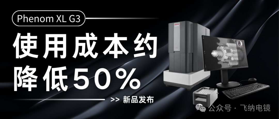
1. New Product Release - Phenom XL G3 Large Warehouse Automated Scanning Electron Microscope
The newly released Phenom XL G3 automated scanning electron microscope, with its 3000 hour long life CeB crystal filament and AI intelligent automation function, has opened a new era of scanning electron microscopy! Whether it's quality control, R&D testing, or precise analysis, Phenom XL G3 will bring improvements to your work.
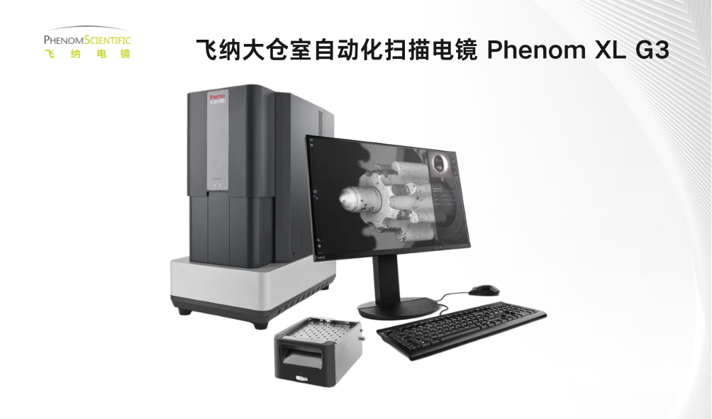
Stable and reliable:80 years of top-notch technological heritage.
Using CeB6 crystal filament:3000 hours of ultra long service life, with an average of 5 years for filament replacement.
Automation and AI intelligent scanning electron microscopy for Industry 4.0:Open programming interface, create customized "black light laboratory" testing process, support Maps based multimodal, multi-dimensional automatic puzzle and association.
Do not choose the installation environment:Built in shock absorption system, can be directly placed in production workshops, high-rise QC laboratories, etc.
Original factory integrated energy spectrum EDS:From electronic optical settings, image acquisition to energy spectrum analysis and surface distribution, all are completed in the same unified and intuitive interface.
Low voltage imaging function:For non-conductive, poorly conductive, and electron beam sensitive samples, imaging capability can still be achieved without spraying gold.
2. Highest resolution - Phenom desktop field emission scanning electron microscope
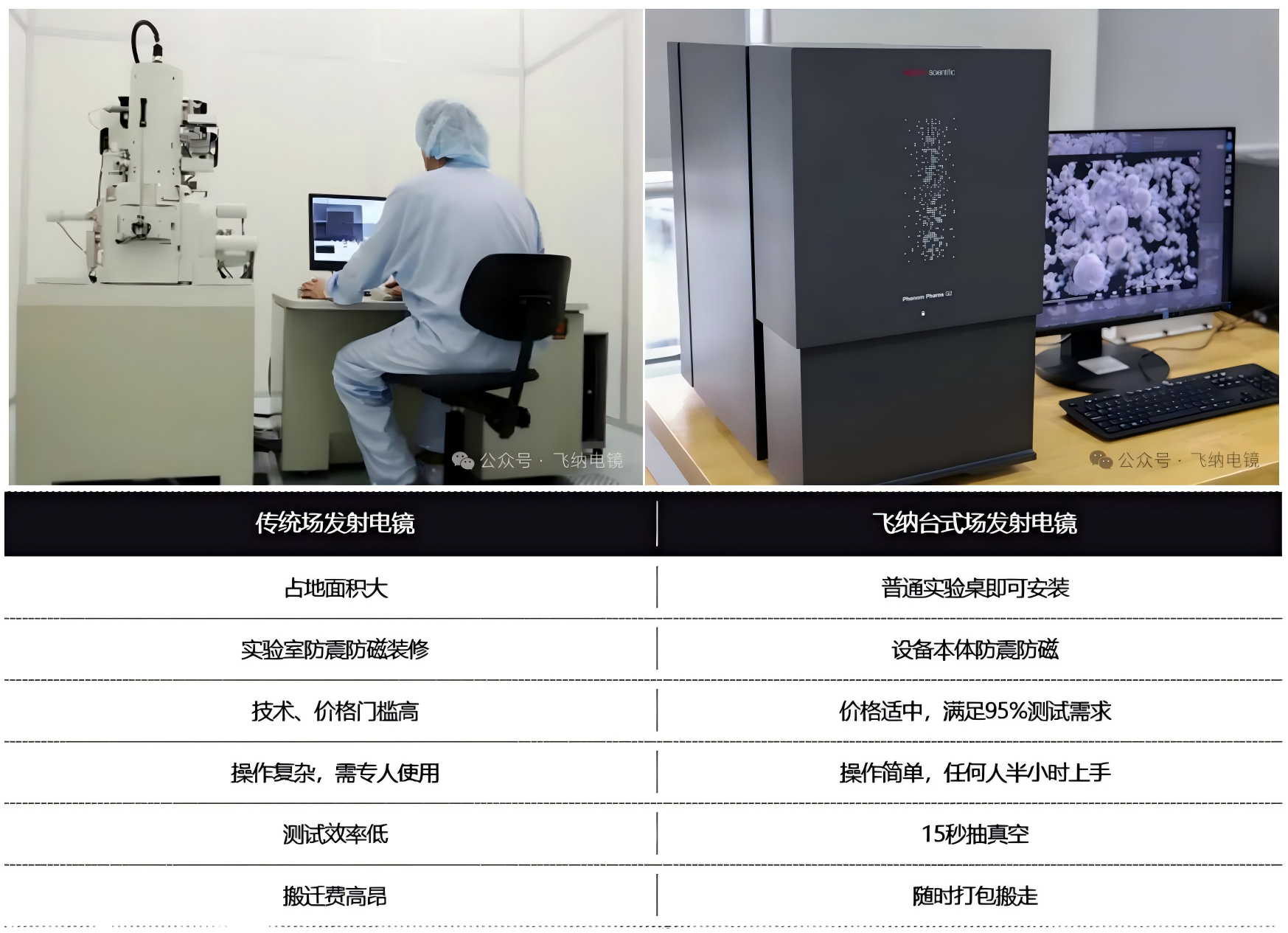
Feina desktop field emission scanning electron microscope, shock resistant, achieves performance close to large-scale field emission on desktop aircraft. Excellent low-voltage imaging capability can reduce the damage and penetration of electron beams on samples, and largely restore the true morphology of samples. Continuing the integrated design of electron microscopy and energy spectrum, the upgraded rapid surface scan can instantly display the distribution of selected elements, and the real-time energy spectrum analysis function greatly improves detection efficiency.
Model recommendation
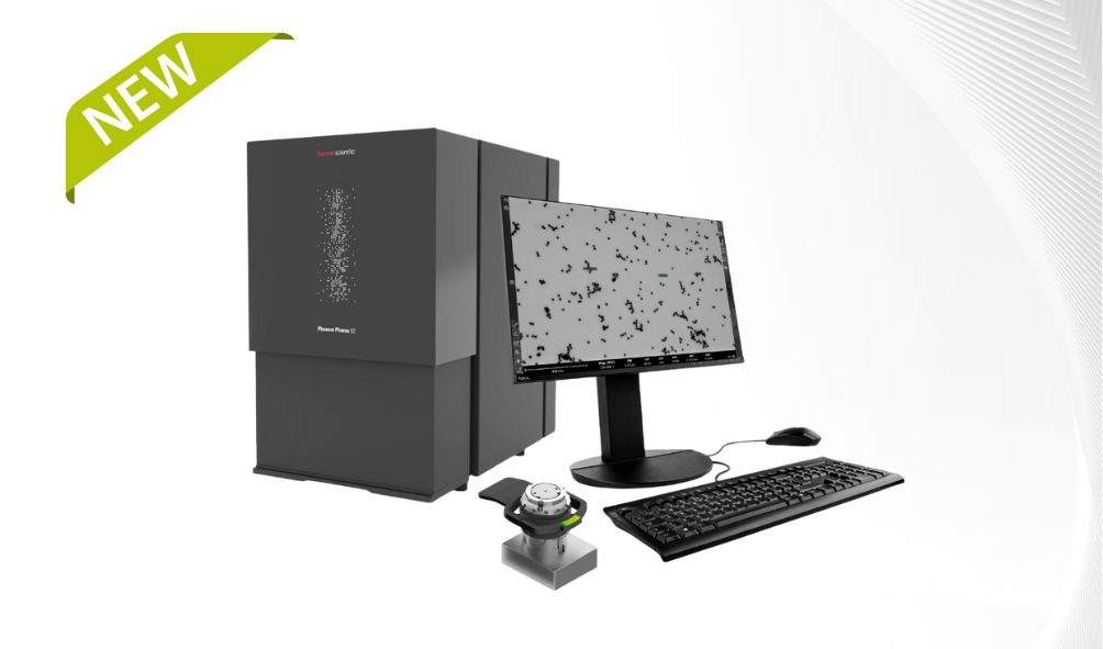
Pharos STEM Scanning Transmission Electron Microscope
Resolution: better than 1nm
Imaging modes: BF, DF, HAADF
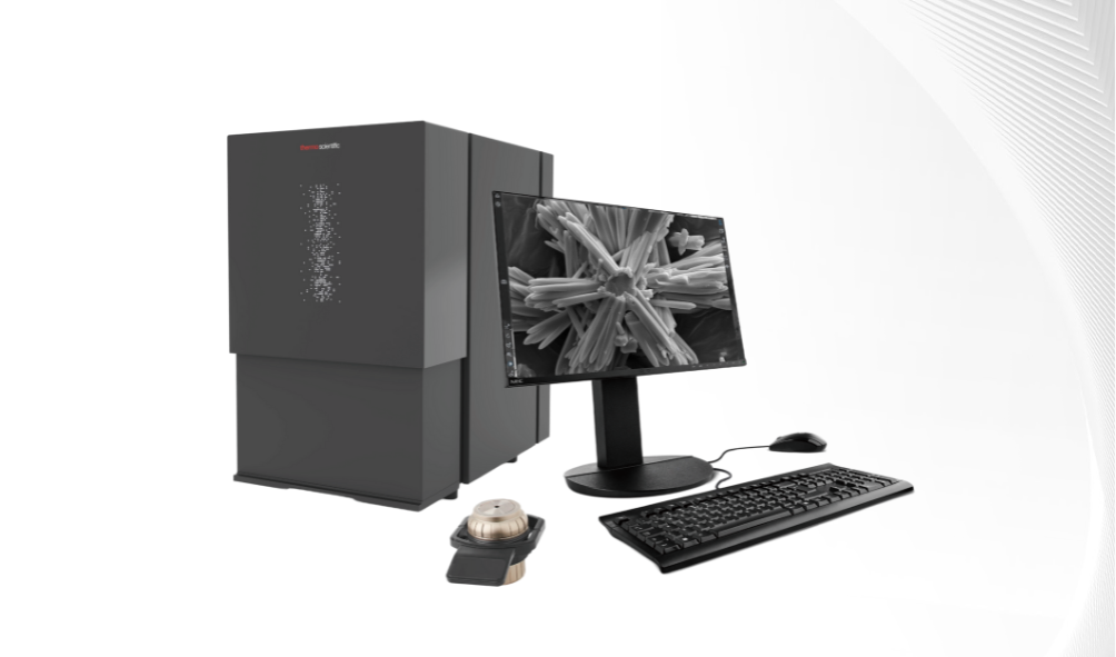
Pharos G2 desktop field emission scanning electron microscope
Resolution: better than 1.5 nm
Magnification factor: 2000000 X
3. AFM-SEM Atomic Force Scanning Electron Microscope
The emergence of AFM in SEM technology combines atomic force microscopy (AFM) with scanning electron microscopy (SEM) to achieve multimodal correlation analysis. It can not only accurately navigate the probe to the region of interest (ROI), but also reliably characterize electrical properties.
Model recommendation(Click on the image to view detailed information)
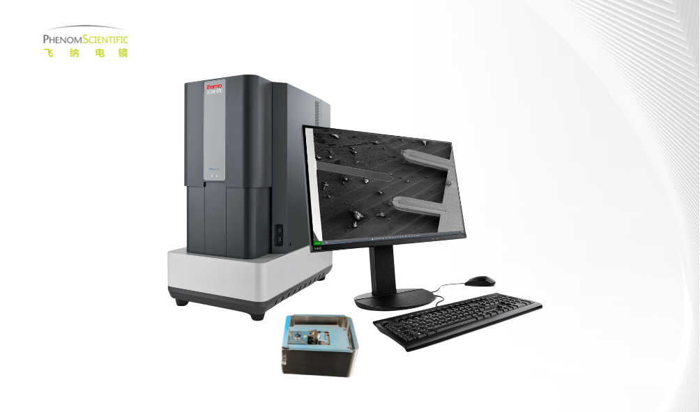
Phenom AFM-SEM
Atomic force scanning electron microscope integrated machine. By combining the advantages of the Feina desktop scanning electron microscope and atomic force microscope, multimodal correlation analysis of samples has been achieved in the same system.
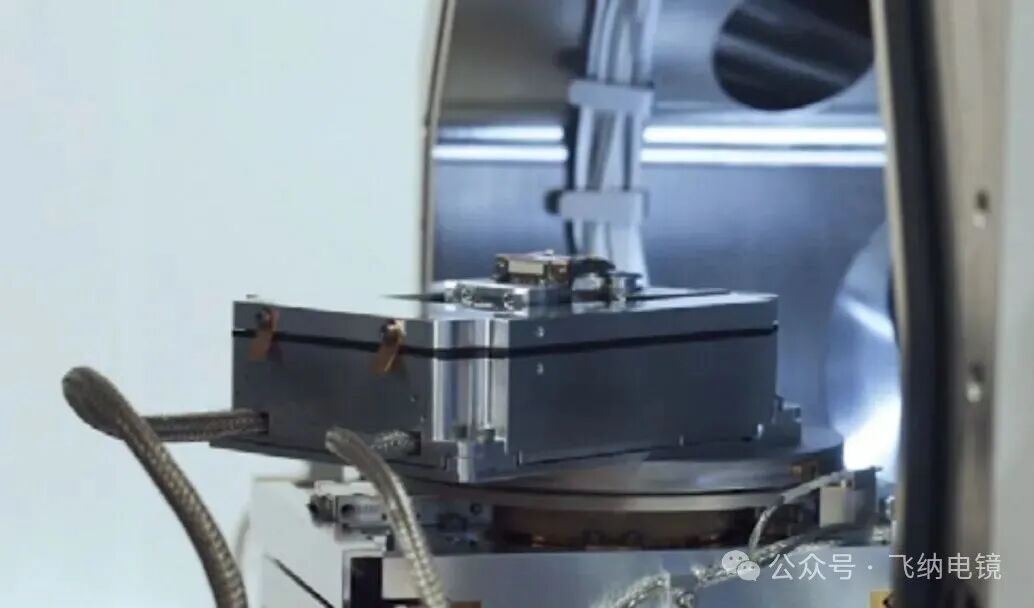
LiteScope AFM-SEM
Synchronized universal technology compatible with Thermo Fisher Scientific TESCAN、 Mainstream brands such as Zeiss, Hitachi, JEOL, etc. have SEM systems, and other brands of electron microscopes can also be customized.
PART.02 Technoorg Linda Sample Preparation
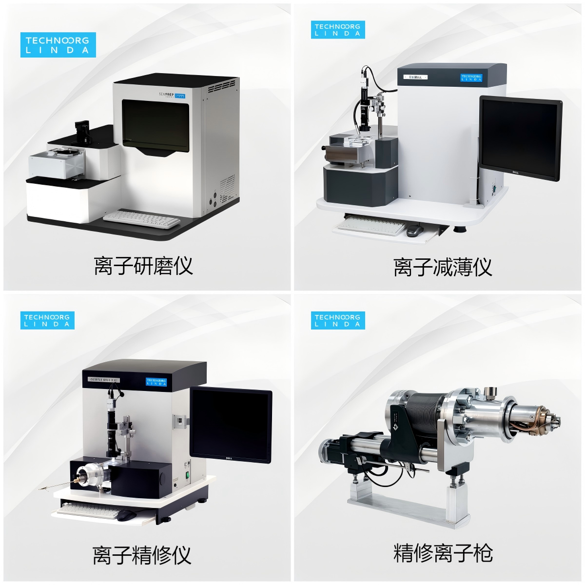
The Technoorg Linda series of ion grinders, ion slicers, and ion polishers are powerful tools for preparing SEM/TEM/XTEM/FIB samples. This series of products adopts ion beam technology, which can perform rapid grinding, surface fine processing, and final polishing on samples. Ion milling system is a high-precision surface treatment technology mainly used in materials science and semiconductor industry. At present, the vast majority of ion milling systems are operated using traditional touch screens or mechanical keyboards. And the latest Technoorg Linda product SEMPREP SMART innovatively adopts an intelligent AI operation mode, which is a conversational ion grinding system!
PART.03DENSsolutions TEM in-situ sample rod
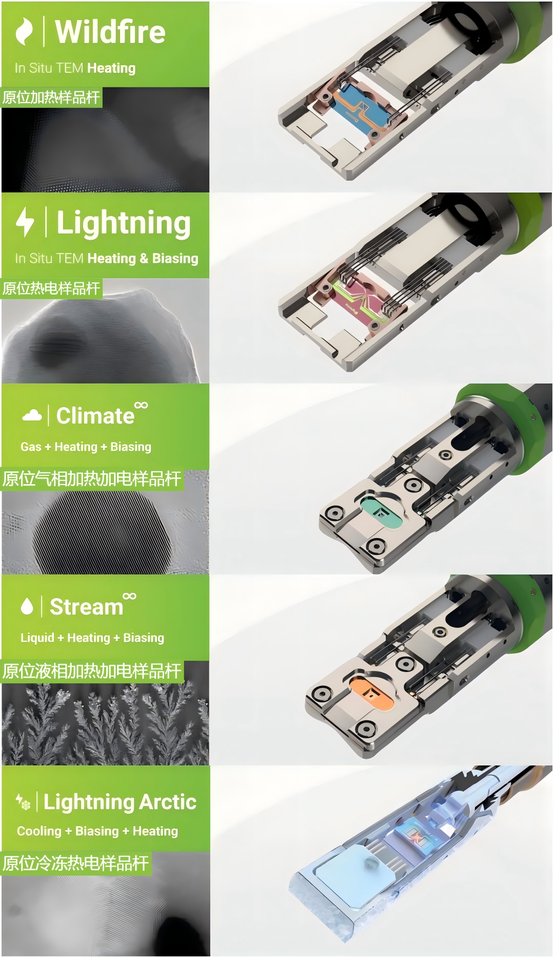
DENSsolutions products can apply external stimuli to in-situ TEM samples and capture the dynamic phenomena of TEM samples in real environments. The four in-situ experimental schemes currently available: Wildfire TEM in-situ heating scheme, Lightning TEM in-situ thermoelectric scheme, Arctic TEM in-situ low-temperature freezing thermoelectric scheme, Climate Infinity TEM in-situ gas-phase heating and electrification scheme, and Stream Infinity TEM in-situ liquid-phase heating and electrification scheme, have opened up possibilities for various disciplines to study various materials and processes under relevant conditions.
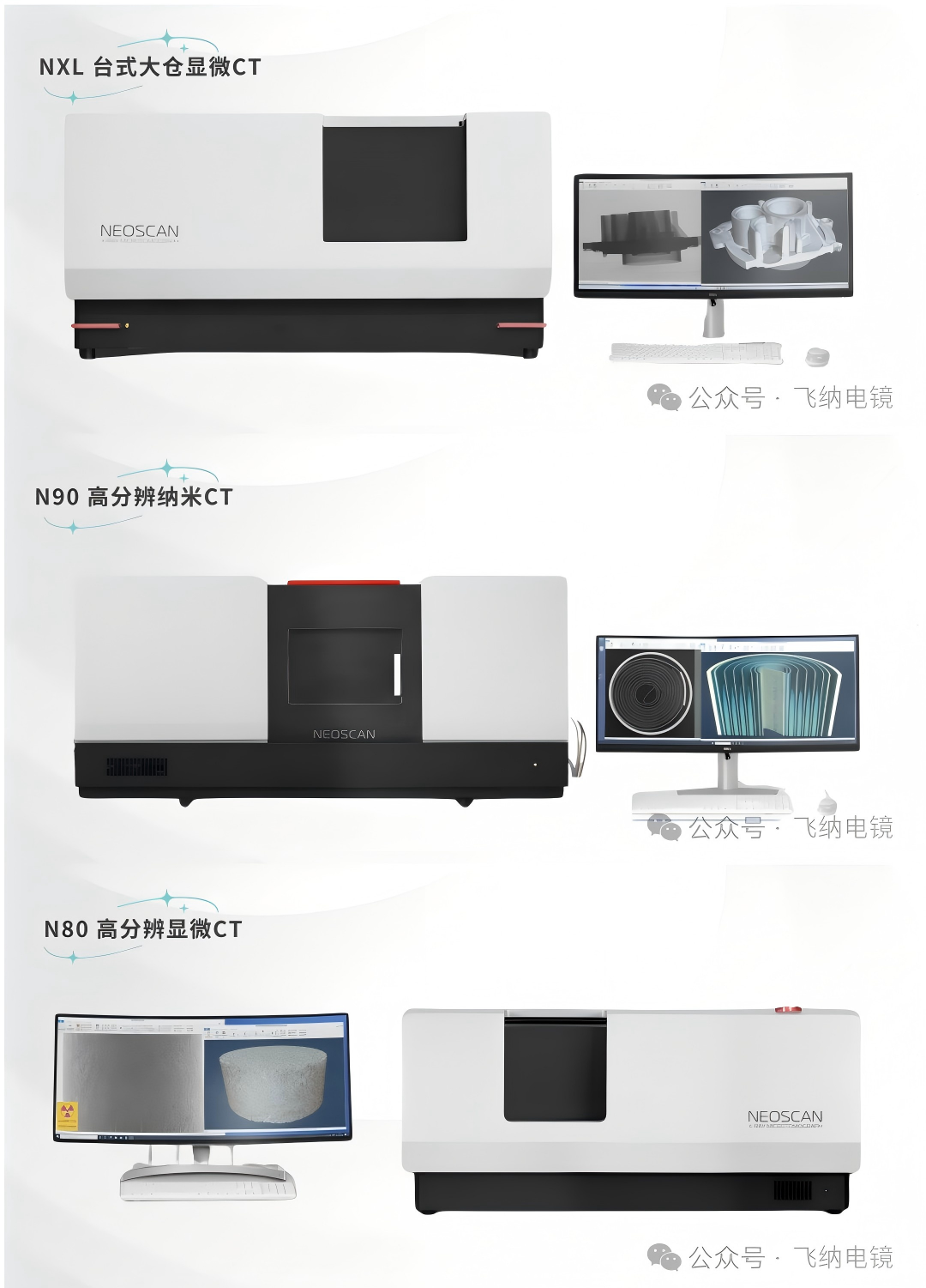
PART.04: The highest resolution desktop micro CT
The NEOSCAN desktop micro CT scanning system requires minimal site requirements, is maintenance free, and has high spatial resolution. The ability to accurately reproduce the internal structure of materials has become an irreplaceable testing method in material research, failure analysis, and process optimization.
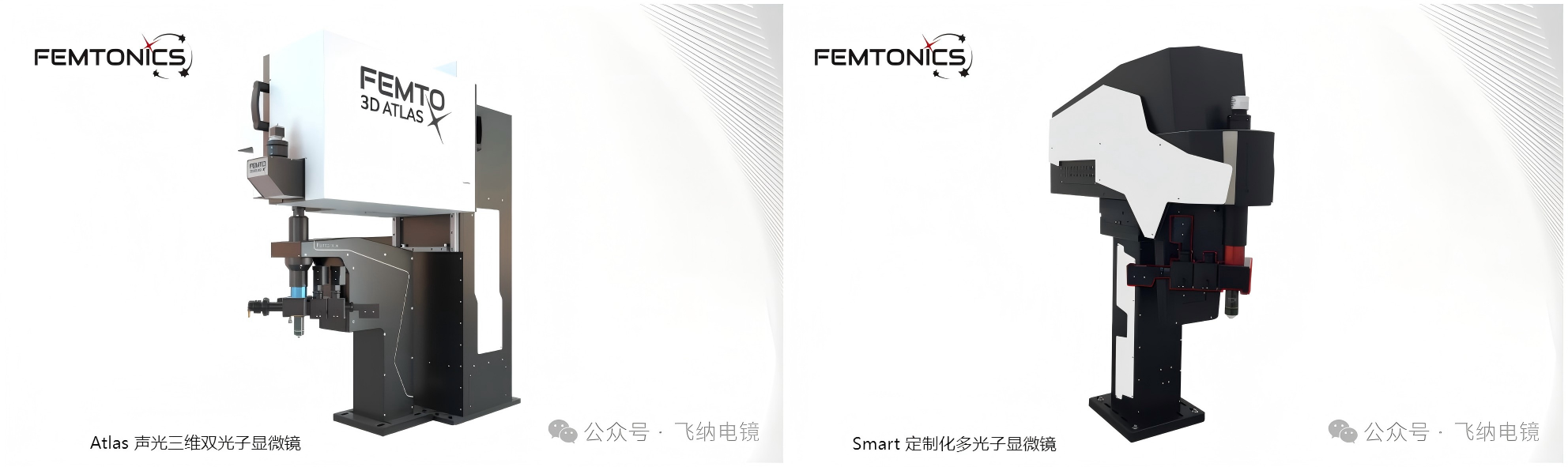
PART.05 FemtonicsTwo-photon microscope
Fermi Optics' two-photon microscopy imaging product is from Budapest, Hungary, dedicated to providing advanced two-photon imaging systems for top researchers worldwide. Atlas acousto-optic 3D two-photon microscope adopts acousto-optic technology and has a scanning speed far higher than market products. 3D random access point scanning speed up to100 kHzThe high-speed arbitrary frame scanning speed is40 fps@510 ×510 pxWhen the target is focused on the field of view, up to3000 fpsIt has already createdMore than 20 world recordsAnd possess44 international patents,Over 200 publications of technological achievementsMost of the results have been published in top journals such as Nature, Science, Cell, and Neuron.
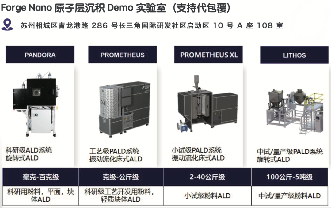
PART.06 Forge Nano Powder Atomic Layer Deposition
Forge Nano adopts atomic layer deposition (ALD) technology, which can provide a complete solution from coating research and development to industrial production, including fluidized bed technology, rotating bed, vibrating bed, etc. By achieving powder processing capacities ranging from milligrams to tons, you can easily implement product development plans from laboratory to production. ALD can be applied to various electrode and electrolyte powder materials, with advantages such as extending battery cycle life, reducing gas generation, reducing irreversible lithium loss, and high voltage stability.
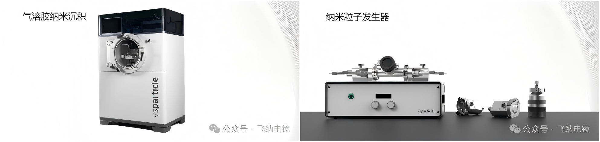
PART.07 VSParticle Nanodeposition System
The VSP-P1 nano printing deposition system can achieve direct printing of inorganic nanostructured materials with unique properties. The particles of the printed coating are generated by the VSP-G1 nanoparticle generator, and the aerosol particles generated by spark ablation have a typical particle size of less than 20nm and do not contain surfactants or any other organic additives. The entire process of nanoparticle production and printing deposition is automated and does not require subsequent heat treatment to remove organic components.