-
E-mail
info@phenom-china.com
-
Phone
18516656178
-
Address
Room T5705, Shanghai Hongqiao Libao Plaza, No. 88 Shenbin Road, Hongqiao Town, Minhang District, Shanghai
Funa Scientific Instruments (Shanghai) Co., Ltd
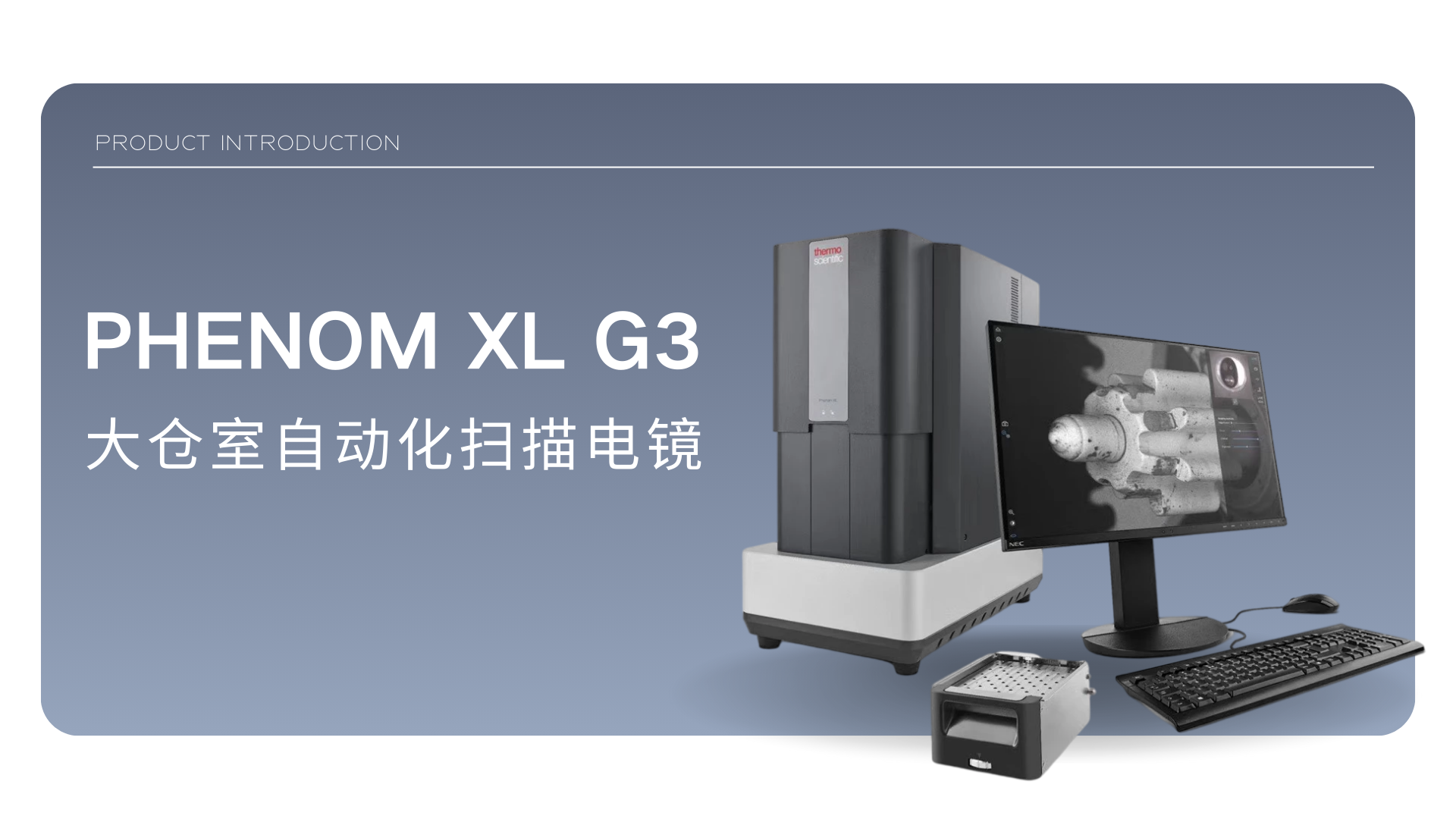
New product release! Scanning Electron Microscope 3000h Filament Heavy Attack! Embark on the Phenom XL G3 era!
Date: 2025-09-08Read: 2
New products are coming! The Phenom XL G3 scanning electron microscope is equipped with a 3000h filament, which is replaced on average every 5 years, making it truly worry free and cost-effective. AI intelligence, automatic puzzle solving, integrated energy spectrum, easily achieve Industry 4.0 level detection. Both research laboratories and production workshops can operate quickly and stably.
Quick Overview of Characteristics
Stable and reliable:80 years of top-notch technological heritage.
Using CeB6Crystal filament:3000 hours of ultra long service life, with an average of 5 years for filament replacement.
Automation and AI intelligent scanning electron microscopy for Industry 4.0:Open programming interface, create customized "black light laboratory" testing process, support Maps based multimodal, multi-dimensional automatic puzzle and association.
Do not choose the installation environment:Built in shock absorption system, can be directly placed in production workshops, high-rise QC laboratories, etc.
Original factory integrated energy spectrum EDS:From electronic optical settings, image acquisition to energy spectrum analysis and surface distribution, all are completed in the same unified and intuitive interface.
Low voltage imaging function:For non-conductive, poorly conductive, and electron beam sensitive samples, without spraying gold, it still has excellent imaging capabilities.
01. Top technology inheritance in 1980
(1) Philips Era (1939-1996)
Origin:In 1939, Le Poole proposed the concept of an electron microscope, and in 1944, he successfully developed a 150kV electron microscope, laying the technical foundation.
development:The first commercial electron microscope EM100 was launched in 1949. Subsequently, innovative products were continuously introduced, such as entering the SEM market in 1972 and launching the PSEM500.
(2) FEI period (1996-2016)
mergeIn 1997, Philips' electronic optics business merged with FEI to acquire ESEM technology, enhancing its technological strength.
Innovation:In 2006, the desktop scanning electron microscope Phenom World was launched, using a 1500h long life CeB6 filament.
(3) Thermo Fisher era (2016 present)
AcquisitionIn 2016, FEI was acquired by Thermo Fisher Scientific. In 2018, Phenom World was acquired by Thermo Fisher Scientific and officially renamed as the Thermo Scientific brand.

Inheritance and Development:Technologically inheriting FEI's innovative achievements, we continue to improve performance. Currently, in addition to the CeB filament series, we also have a desktop field emission electron microscope series, specialized electron microscopes for specific fields such as public security and forensic medicine, with a rich product line and dozens of models.
From Philips to Thermo Fisher, the Feina electron microscope has undergone nearly 80 years of technological accumulation, from its initial concept and commercialization to continuous technological innovation and breakthroughs, always maintaining a leading position in the field of electron microscopy.
02.3000h CeB6 Crystal filament - replace filament every 5 years on average
Equipped with ultra long lifespan core components, using 3000 hours of high brightness cerium hexaboride (CeB ₆) filament, the filament is replaced on average every 5 years, ensuring continuous operation of the equipment 7 × 24 hours, reducing maintenance frequency and holding costs, and ensuring worry free long-term stable operation of production lines or laboratories.
03. AI Intelligent Scanning Electron Microscope - Automation for Industry 4.0
From sample loading to image output, it only takes 1 minute, with high testing efficiency. Operators do not need to wait for long periods of time, and the detection flux is 5-10 times higher than traditional electron microscopes, greatly accelerating QC judgment and R&D iteration.
(1) Deep integration, on-demand change
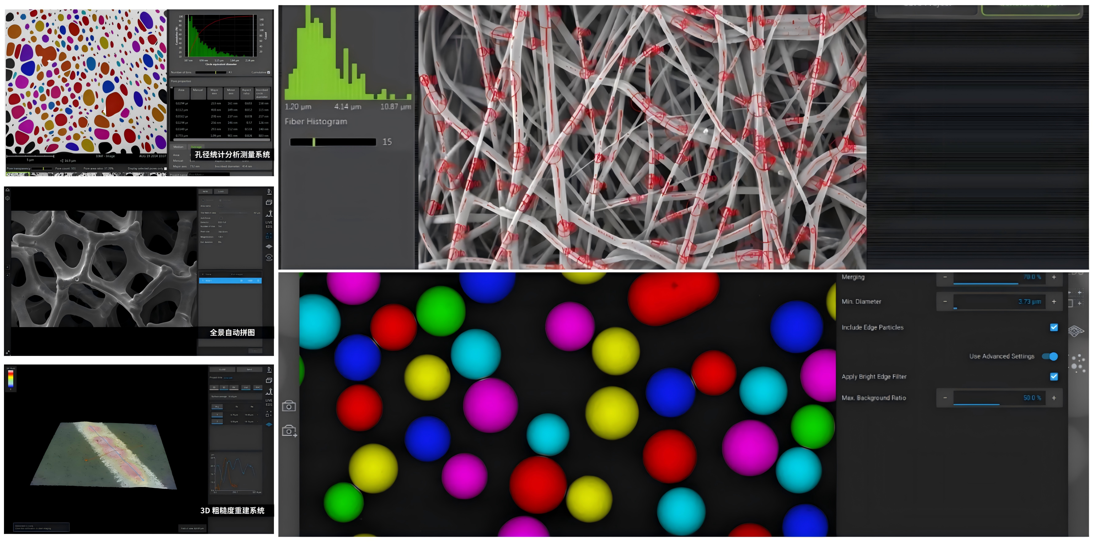
An open automation interface that provides Python script control (PPI) that can be seamlessly integrated into customers' existing automated production lines and LIMS systems. A precise automated motor table, combined with software scripts, can accommodate 36 samples at a time, creating an "unmanned quality inspection factory". Customized programs can automatically take photos and analyze large quantities of samples at night or during rest time, maximizing equipment utilization.
(2)View the whole picture with one image, analyze multiple points without omission
Automatically obtain panoramic high-definition images on large samples such as wafers, filter membranes, and metal fracture surfaces, and perform high magnification analysis on preset key points to ensure no blind spots during detection.
(3)From 'seeing' to 'calculating'
Professional automated analysis software, specialized software such as ParticleMetric and FiberMetric. Automated completion of statistical tasks such as particle size, morphology, and size distribution that require several hours of manual labor, outputting standardized reports, and achieving true quantitative quality control.
04 Do not choose installation environment
Built in shock absorption system, environmental adaptability
Built in shock absorption system, low installation environment requirements, no need for shock absorbers, can be directly placed in production workshops, floor QC laboratories, etc., and can even be used in vehicles and outdoor scenes. Save laboratory renovation costs and truly achieve the goal of 'affordable and better use'.
The Funa electron microscope has participated in scientific research projects such as Iceland's volcanic crater and Spain's uninhabited island, and is a portable scanning electron microscope suitable for harsh environments. Researchers collected samples and returned them to the tent, using a Funa electron microscope to determine the chemical composition of the samples, greatly improving the efficiency of sample collection and analysis.

05. Original factory integrated energy spectrum EDS
Integrated energy spectrum detector, all operations from electronic optical settings, image acquisition to energy spectrum analysis and surface distribution are completed in the same unified and intuitive interface.
(1) ChemiSEM Color Imaging Technology
Real time synchronization of morphology images and element data, seamless calling. Users can perform point, line, and surface analysis in real-time while observing the morphology, without the need for any data import or export steps.
(2)Phase Mapping software for phase analysis
The proprietary online phase analysis software module (Phase Mapping) utilizes powerful algorithms to automatically identify, classify, and calibrate different "phases" or "compounds" based on the quantitative results of each pixel element.
06. Low voltage imaging function
The PhenomXL G3 is equipped with a newly upgraded vacuum design and backscatter detector (BSD), optimizing sensitivity at low voltages and improving overall signal-to-noise ratio (S/N). For non-conductive, poorly conductive, and electron beam sensitive samples, lower beam currents can be used for shooting, improving resolution while reducing the impact of charge effects.
Due to the overall improvement in signal-to-noise ratio, we can capture photos of the same quality in a shorter acquisition time. In the automated workflow, the overall efficiency of high-throughput photo shooting is increased by an average of 30%.
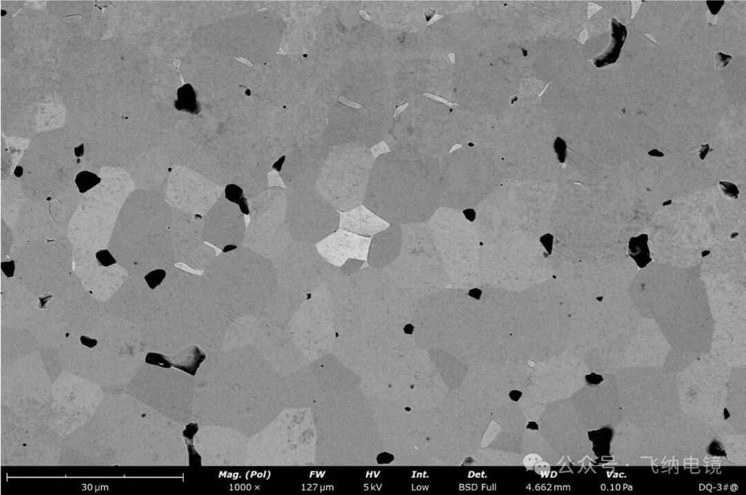
Electronic ceramics
Magnification factor: 1000X
5kV, Unprayed gold, backscattered electron image
Observing the grain size and voids inside the ceramic
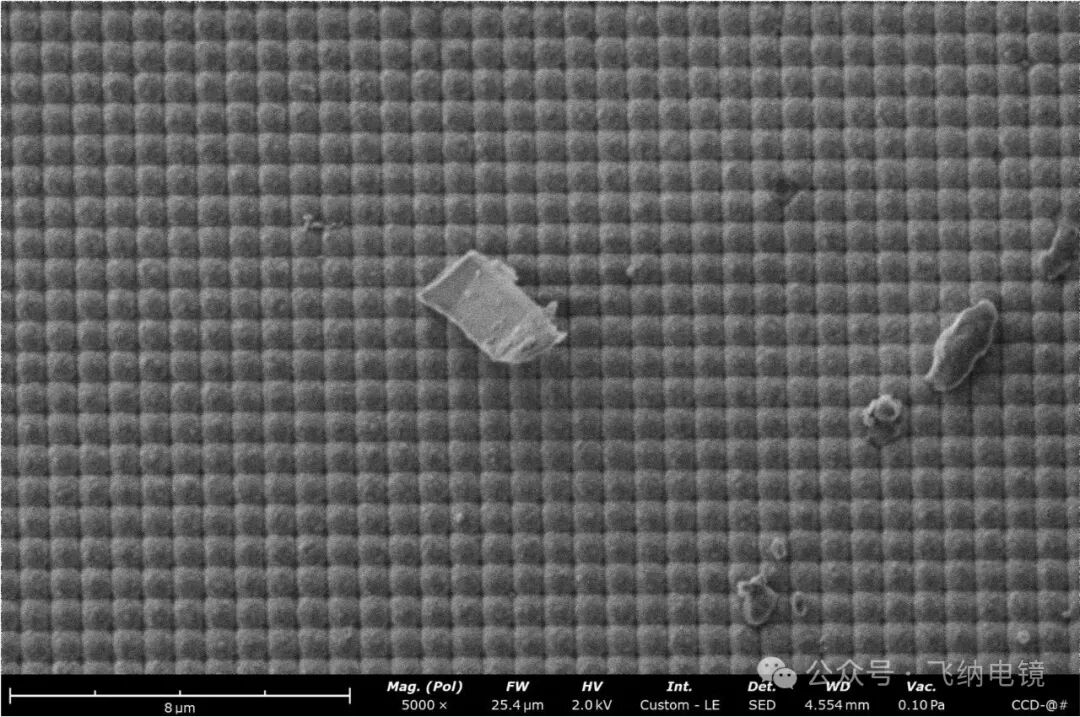
CMOS detector
Magnification factor: 5000X
2kV, Secondary electron image
Clear visibility of pixel units and surface pollutants