-
E-mail
sales@opton.com.cn
-
Phone
13126536208
-
Address
Oubotong Group, Building 2, No. 1100 Huihe South Street, Chaoyang District, Beijing
Beijing Obotong Optical Technology Co., Ltd
The working principle and application fields of SEM scanning electron microscope
Date: 2025-10-20Read: 2
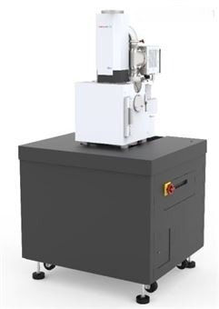
SEM scanning electron microscope is a high-resolution microscope that uses an electron beam to scan the surface of a sample and obtains the microstructure of the sample by detecting the signals generated by the interaction between the sample surface and the electron beam. Its high-resolution imaging capability and multifunctional analysis characteristics make it play an important role in scientific research and industrial testing.
1、 Working principle
SEM scanning electron microscopeThe basic working principle is to scan the surface of the sample with an electron beam, and then form an image by detecting the signals reflected back from the sample surface (including secondary electrons, backscattered electrons, X-rays, etc.). This process can be divided into the following steps:
1. Electron source: Electron sources typically use hot cathodes or field emission cathodes to generate high-energy electron beams. These electron beams become very fine through a focusing system and can be scanned at the micrometer or nanometer scale.
2. Scanning process: The electron beam scans the sample surface according to certain rules, usually using point scanning method. Every time a point is scanned, the sample interacts with electrons, resulting in different types of signals. These signals are received by detectors and corresponding images are generated based on the strength and changes of the signals.
3. Signal detection: During the scanning process, the sample surface will release secondary electrons, backscattered electrons, X-rays, etc. The secondary electrons mainly come from the surface of the sample, and their quantity is related to the detailed structure of the sample surface. Therefore, the surface morphology image of the sample can be obtained through the secondary electron signal; Backscattered electrons can provide atomic number information of the sample, which can be used to identify the composition distribution of different materials; X-rays provide chemical composition information of the sample through elemental analysis.
4. Image reconstruction: The detected signals are processed by the computer system of an electron microscope and converted into grayscale images, displaying the microstructure of the sample surface. In SEM images, the height and shape of the sample are presented through secondary electron signals of different intensities. The more concave the part, the weaker the secondary electron signal, indicating darker areas. The more prominent the part, the stronger the signal, indicating brighter areas.
2、 Application Fields
Due to its high resolution, high magnification, and ability to reconstruct three-dimensional morphology, SEM scanning electron microscopy has been widely used in multiple fields
1. Materials Science: In materials research, it is widely used to observe the microstructure, surface morphology, fracture mechanism, corrosion analysis, etc. of materials such as metals, ceramics, semiconductors, polymers, etc. For example, SEM can be used to observe cracks on metal surfaces, the structure of welded joints, and the coating quality of metal materials.
2. Life sciences: Their applications in biological research are also very extensive, especially in the fields of cytology and microbiology. SEM can clearly observe the surface structure of cells, such as cell membrane, extracellular matrix, virus surface, etc. By using it, researchers can conduct detailed analysis of the subtle structures of pathogens, viruses, and cellular tissues.
3. Electronics and Semiconductor Industry: In the electronics industry, it is used in the manufacturing process of integrated circuits (ICs), electronic devices, optical fibers, etc. to detect their surface structure and production quality. Especially in the research of semiconductor materials, nanoscale defects, fractures, and poor contacts can be revealed, providing a basis for improving manufacturing processes.
4. Geology and Mineralogy: In mineralogy, it is used to study the surface morphology of rocks and minerals, the microstructure of minerals, and the chemical composition of ores. Through backscattered electron images, geologists can analyze the composition and types of minerals in ores based on the distribution of different elements.
SEM scanning electron microscope, with its excellent resolution and multifunctionality, is widely used in scientific research and industrial production, especially in fields such as materials science, biomedicine, electronics industry, and nanotechnology. It scans the surface of the sample with a high-energy electron beam, detects different signals to obtain fine microscopic images, and provides important information about the chemical composition, physical properties, and other aspects of the sample.