-
E-mail
sales@opton.com.cn
-
Phone
13126536208
-
Address
Oubotong Group, Building 2, No. 1100 Huihe South Street, Chaoyang District, Beijing
Beijing Obotong Optical Technology Co., Ltd
Application of Focused Ion Beam Microscopy in Materials Science
Date: 2025-10-17Read: 2
Focused ion beam microscopy is an important analytical tool in materials science, which combines scanning electron microscopy (SEM) and ion beam technology and is widely used for material characterization, microfabrication, and three-dimensional structure analysis. It can accurately observe and process materials at the nanoscale, which is of great significance for understanding the microstructure and properties of materials.
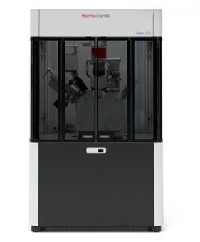
Focused ion beam microscopeThe applications in materials science are mainly reflected in the following aspects:
1、 Analysis of Material Surface and Microstructure
One common application is to characterize the microstructure of materials. It can provide high-resolution images and clearly observe nanoscale surface morphology, microstructure, and defects. For example, in the study of metal materials, the distribution of grain boundaries, phase boundaries, and grains can be observed, which is of great significance for studying the mechanical properties and corrosion resistance of materials.
2、 3D Structure Reconstruction and Tomography
By using the layer by layer cutting function, the three-dimensional structural information of the sample can be obtained. It is also possible to perform micro cutting of samples, remove materials layer by layer, and combine imaging technology to achieve 3D reconstruction. This technology has important applications in the research of nanomaterials, composite materials, and multilayer structures, which can help researchers reveal the internal structure of complex materials. For example, in the research of lithium battery materials, it is possible to reveal the structural changes of electrode materials during charge and discharge processes.
3、 Microfabrication and Nanomanufacturing
Focused ion beam microscopy is not only capable of observing material surfaces, but also has the ability for microfabrication. By precise control of the focused ion beam, materials can be cut, carved, and processed at the nanoscale. In the fields of microelectronics and nanomanufacturing, it can be used to create microchannels, mask patterns, microstructures, and microdevices. For example, in semiconductor device manufacturing, it can be used to process small structures for fault analysis and circuit repair.
4、 Material defect analysis and fault location
It can accurately reveal micro defects in materials, such as cracks, pores, inclusions, and metal brittleness. Through high-resolution imaging, the distribution of these defects and their impact on material properties can be observed at the nanoscale. In addition, it can be combined with other analytical techniques such as energy dispersive X-ray spectroscopy (EDX) for elemental analysis to help locate the cause of faults, especially in fields such as aerospace and automotive industry, where it is an important tool for fault diagnosis.
5、 Element distribution and composition analysis
Combined with energy spectrum analysis, qualitative and quantitative analysis of material elements can be provided. In materials science, understanding the elemental distribution and chemical composition of materials is crucial for optimizing material properties. Through precise processing, local analysis of the sample can be conducted to reveal the distribution of different elements in the material. For example, in the study of composite or alloy materials, the microscopic distribution of different components and their impact on material properties can be revealed.
The application of focused ion beam microscopy in materials science is very extensive, especially in the fields of nanomaterials, composite materials, semiconductors, etc. It has important research value. It not only provides high-resolution surface imaging, but also has various functions such as microfabrication, 3D reconstruction, and elemental analysis, making it an important tool for material characterization, microfabrication, and fault analysis.