- Phone
-
Address
5th Floor, Helen International Building, 778 Baoshan Road, Hongkou District, Shanghai
Product Categories
Shanghai Juna Technology Co., Ltd

confocal laser scanning microscope
NegotiableUpdate on 05/06
- Model
- Nature of the Manufacturer
- Producers
- Product Category
- Place of Origin
Overview
Laser confocal scanning microscope achieves real-time confocal microscopy images through a fast optical scanning module and signal processing algorithm. We have solutions for measuring and detecting micro three-dimensional structures, such as semiconductor chips, FPD products, MEMS devices, glass substrates, material surfaces, and more.
Product Details
confocal laser scanning microscopeIt is an accurate and reliable three-dimensional (3D) scanning system that achieves real-time confocal microscopy images through fast optical scanning modules and signal processing algorithms. We have * * solutions for measuring and detecting micro 3D structures, such as semiconductor chips, FPD products, MEMS devices, glass substrates, material surfaces, etc.
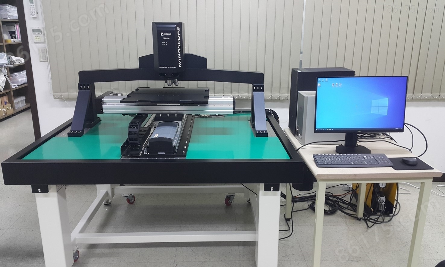
Features&Benefits:
High resolution non-destructive optical 3D measurement with automatic tilt compensation
Real time confocal imaging simple data analysis mode
Multiple optical zoom dual Z-scan
Feature detection of large-scale splicing of semi transparent substrates
Real time CCD bright field and confocal imaging without sample preparation
autofocus
Application field:
NS-3500 is a promising solution for measuring low dimensional materials.
Can measure the height, width, angle, area, and volume of micrometer and submicron structures, such as
-Semiconductor: IC graphics, bump height, coil height, defect detection, CMP process
-FPD products: touch screen detection, ITO pattern, LCD pillar spacing height
-MEMS devices: 3D structural profile, surface roughness, MEMS graphics
-Glass surface: thin-film solar cells, solar cell textures, laser patterns
-Material research: Mold surface inspection, roughness, crack analysis
Specification(confocal laser scanning microscopeSpecification:
| Model | Microscope NS-3500 | remark | |||||
| Controller NS-3500E | |||||||
| Objective magnification | 10x | 20x | 50x | 100x | 150x | ||
| Observation/measurement range | Horizontal (H): μ m | 1400 | 700 | 280 | 140 | 93 | |
| 垂直 (V): μm | 1050 | 525 | 210 | 105 | 70 | ||
| Scope of work: mm | 16.5 | 3.1 | 0.54 | 0.3 | 0.2 | ||
| Numerical aperture (N.A.) | 0.30 | 0.46 | 0.80 | 0.95 | 0.95 | ||
| optical zoom | x1 to x6 | ||||||
| Total magnification | 178x to 26700x | ||||||
| Observation/measurement optical system | Pinhole confocal optical system | ||||||
| height measurement | Measurement scanning | Long scan: 10mm | |||||
| display resolution | 0.001 μm | ||||||
| Repetition rate σ | 0.010 μm | Note 1Measure the standard sample (with a step size of 1 μ m) 100 times using a 100 ×/0.95 objective lens. | |||||
| Width measurement | display resolution | 0.001 μm | |||||
| Repetition rate 3 σ | 0.02 μm | Note 2Measure the standard sample (5 μ m spacing) 100 times with a 100 ×/0.95 objective lens | |||||
| Frame memory | pixel | 1024x1024, 1024x768, 1024x384, 1024x192, 1024x96 | |||||
| Monochrome image | 12 bit | ||||||
| color image | 8-bit for RGB each | ||||||
| height measurement | 16 bit | ||||||
| frame rate | Surface scanning | 20 Hz to 160 Hz | |||||
| Line scanning | ~8 kHz | ||||||
| automatic function | automatic gain | ||||||
| Laser confocal measurement light source | wavelength | 405nm | |||||
| output | ~2mW | ||||||
| Laser grade | Class 3b | ||||||
| Laser receiving element | PMT (Photomultiplier Tube) | ||||||
| Optical observation light source | lamp | 10W LED | |||||
| Optical observation camera | imaging element | 1/2 "color image CCD sensor | |||||
| Record resolution | 640x480 | ||||||
| auto-adjust | Gain, Shutter Speed, White Balance | ||||||
| Data processing unit | PC | ||||||
| power supply | power supply voltage | 100 to 240 VAC, 50/60 Hz | |||||
| Current consumption | 500 VA max. | ||||||
| weight | microscope | Approx. ~200 kg (Measuring head unit : ~12 kg) | |||||
| controller | ~8 kg | ||||||


