- Phone
-
Address
5th Floor, Helen International Building, 778 Baoshan Road, Hongkou District, Shanghai
Product Categories
Shanghai Juna Technology Co., Ltd

NS3500 G Large Non Contact 3D Laser Scanner
NegotiableUpdate on 05/06
- Model
- Nature of the Manufacturer
- Producers
- Product Category
- Place of Origin
Overview
NS-3500G is a reliable 3D non-contact scanner. Real time confocal microscopy images are achieved through fast optical scanning modules and signal processing algorithms. We have * * solutions for measuring and detecting micro 3D structures, such as semiconductor chips, FPD products, MEMS devices, glass substrates, material surfaces, etc.
Product Details
NS3500G Large Non Contact 3D Laser Scanner
NS-3500GIt is a reliable 3D non-contact scanner.Real time confocal microscopy images are achieved through fast optical scanning modules and signal processing algorithms. We have * * solutions for measuring and detecting micro 3D structures, such as semiconductor chips, FPD products, MEMS devices, glass substrates, material surfaces, etc.
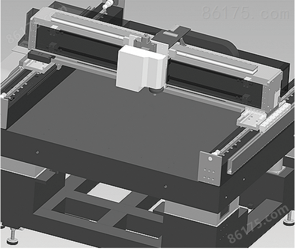
Features & Benefits(Performance and advantages):
High resolution non-destructive optical 3D measurement with automatic tilt compensation
Real time confocal imagingSimple data analysis mode
-
Multiple optical zoom optionsDouble Z-scan
Large scale splicingFeature detection of semi transparent substrates
real-timeCCD bright field and confocal imagingNo sample preparation
autofocus
Application field(Application field):
NS-3500 is a promising solution for measuring low dimensional materials.
Can measure the height, width, angle, area, and volume of micrometer and submicron structures, such as
-Semiconductor: IC graphics, bump height, coil height, defect detection, CMP process
-FPD products: touch screen detection, ITO pattern, LCD pillar spacing height
-MEMS devices: 3D structural profile, surface roughness, MEMS graphics
-Glass surface: thin-film solar cells, solar cell textures, laser patterns
-Material research: Mold surface inspection, roughness, crack analysis
Specification:
Model |
Microscope NS-3500 |
remark |
|||||
Controller NS-3500E |
|||||||
Objective magnification |
10x |
20x |
50x |
100x |
150x |
||
Observation/measurement range |
Horizontal (H): μ m |
1400 |
700 |
280 |
140 |
93 |
|
垂直 (V): μm |
1050 |
525 |
210 |
105 |
70 |
||
Scope of work: mm |
16.5 |
3.1 |
0.54 |
0.3 |
0.2 |
||
Numerical aperture (N.A.) |
0.30 |
0.46 |
0.80 |
0.95 |
0.95 |
||
optical zoom |
x1 to x6 |
||||||
Total magnification |
178x to 26700x |
||||||
Observation/measurement optical system |
Pinhole confocal optical system |
||||||
height measurement |
Measure scanning range |
Long scan: 10mm [NS-3500-T] |
|||||
display resolution |
0.001 μm |
||||||
Repetition rate σ |
0.010 μm |
Note 1 |
|||||
Width measurement |
display resolution |
0.001 μm |
|||||
Repetition rate 3 σ |
0.02 μm |
Note 2 |
|||||
Frame memory |
pixel |
1024x1024, 1024x768, 1024x384, 1024x192, 1024x96 |
|||||
Monochrome image |
12 bit |
||||||
color image |
8-bit for RGB each |
||||||
height measurement |
16 bit |
||||||
frame rate |
Surface scanning |
20 Hz to 160 Hz |
|||||
Line scanning |
~8 kHz |
||||||
automatic function |
automatic gain |
||||||
Laser confocal measurement light source |
wavelength |
405nm |
|||||
output |
~2mW |
||||||
Laser grade |
Class 3b |
||||||
Laser receiving element |
PMT (Photomultiplier Tube) |
||||||
Optical observation light source |
lamp |
10W LED |
|||||
Optical observation camera |
imaging element |
1/2 "color image CCD sensor |
|||||
Record resolution |
640x480 |
||||||
auto-adjust |
Gain, Shutter Speed, White Balance |
||||||
Data processing unit |
PC |
||||||
power supply |
power supply voltage |
100 to 240 VAC, 50/60 Hz |
|||||
Current consumption |
500 VA max. |
||||||
weight |
microscope |
Approx. ~200 kg (Measuring head unit : ~12 kg) |
|||||
controller |
~8 kg |
||||||
Note 1: Conduct 100 measurements on a standard sample (with a step size of 1 μ m) using a 100 ×/0.95 objective lens
Note 2: Conduct 100 measurements on the standard sample (5 μ m spacing) using a 100 ×/0.95 objective lens.


