- Phone
-
Address
Fuxing Industrial Park, Chuangye 1st Road, Jiangbian, Songgang Town, Bao'an District, Shenzhen City
Product Categories
Shenzhen Enyang Technology Co., Ltd


Wafer testing equipment
NegotiableUpdate on 05/14
- Model
- Nature of the Manufacturer
- Producers
- Product Category
- Place of Origin
Overview
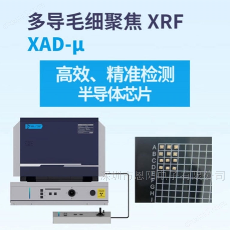
Wafer testing equipment is one of the key devices in the semiconductor manufacturing process, mainly used for electrical performance testing and quality evaluation of integrated circuits (ICs) at the wafer level. With the continuous advancement of microelectronics technology, equipment has also developed in terms of wafer size, testing speed, and accuracy, becoming an important link in modern semiconductor production lines.
Product Details
I. Overview
Wafer testing equipment is one of the key devices in the semiconductor manufacturing process, mainly used for electrical performance testing and quality evaluation of integrated circuits (ICs) at the wafer level. With the continuous advancement of microelectronics technology, equipment has also developed in terms of wafer size, testing speed, and accuracy, becoming an important link in modern semiconductor production lines.
2、 Working principle
The working principle of wafer testing equipment mainly includes the following steps:
1. Wafer loading: Load the wafer to be tested onto the working platform of the testing equipment, usually using vacuum suction or mechanical clamping to fix the wafer in the testing position.
2. Probe Alignment: Using a high-precision positioning system, align the test probe with the test point on the crystal circle. The probe is moved by a robotic arm to ensure accurate contact at each testing point.
3. Signal testing: Use built-in testing instruments and circuits to test the electrical performance of each chip on the wafer. The testing content includes DC testing (such as current, voltage) and AC testing (such as frequency, gain, etc.).
4. Data collection and analysis: During the testing process, the equipment collects real-time data such as current and voltage, and analyzes these data through embedded software to generate test reports, which are provided to engineers for subsequent analysis.
5. Result recording and classification: Based on the test results, classify the good and bad products, and store the data in the database for subsequent tracking and analysis.
3、 Equipment structure
The structure of wafer testing equipment usually consists of the following main parts:
1. Rack: The outer shell structure of the equipment, providing stable support.
2. Testing platform: A workspace used for loading wafers, typically equipped with a vacuum loading system to ensure wafer stability.
3. Probe card: composed of multiple probes, the probes make contact with the wafer surface through spring force to complete electrical measurement.
4. Control system: The core control system is responsible for the operation and data collection of the equipment, and is connected to external computers.
5. Testing instruments: Built in multifunctional testing instruments are responsible for conducting electrical performance tests, usually including DC testers, spectrum analyzers, etc.
6. Software interface: A user interface used for device control, data analysis, and report generation, usually designed with graphics for easy use by operators.
4、 Product Features
4.1high precision
Equipped with a high-resolution positioning system and high-sensitivity probes, it can ensure accurate alignment and precise measurement of test points, reducing testing errors.
4.2High speed testing
With the development of semiconductor devices towards miniaturization and high integration, the testing speed of wafer equipment is also constantly improving. The parallel testing capability and fast switching function of the equipment can complete a large number of testing tasks in a short period of time, improving production efficiency.
4.3Flexibility and Scalability
It usually has good flexibility and scalability, supporting multiple testing modes and different types of probe cards to meet the testing needs of different types of chips.
4.4intelligentization
With the development of artificial intelligence and big data technology, many devices have begun to integrate intelligent analysis functions, which can analyze test data in real time, automatically identify defects, and improve the effectiveness of testing.
4.5人性化界面
Equipment often adopts a user-friendly interface, providing simple operation procedures and clear data display, making it convenient for operators to effectively manage and monitor.
5、 Operation process
5.1 Preparation work
1. Check the equipment status: Ensure that the equipment is operating normally, check the power connection, air pressure, vacuum degree, etc.
2. Loading wafers: Carefully place the wafers to be tested on the testing platform to ensure accurate positioning.
5.2 Setting Test Parameters
1. Choose the testing type: Select the corresponding testing program based on the type of chip that needs to be tested.
2. Set test conditions: Input the required test parameters such as voltage, current, frequency, etc.
5.3 Start testing
1. Run the testing program: Start the testing program, and the device will automatically perform probe positioning, signal testing, and data acquisition.
2. Real time monitoring: Operators can monitor the testing process in real time through the display interface, adjust testing parameters at any time to ensure testing quality.
5.4 Data Analysis and Report Generation
1. Data processing: After the test is completed, the collected data information will be automatically uploaded to the computer for analysis.
2. Generate report: The system generates a detailed test report based on the test results, including qualified and unqualified troubleshooting.
5.5 End of Test
1. Remove the wafer: After the test is completed, safely remove the wafer and clean the equipment.
2. Record data: Save test records for subsequent tracking analysis and quality control.
6、 Application Fields
6.1 Semiconductor Manufacturing
Wafer testing equipment is a core link in the semiconductor production process, used to ensure that the electrical performance of integrated circuits on each wafer meets design standards and guarantees product quality.
6.2 Research and Development Laboratory
In semiconductor research and development, it is used to verify the electrical properties of new materials, structures, and processes, promoting technological progress and innovation.
6.3 Material Analysis
Research institutions conduct in-depth studies on the electrical properties of specific materials through equipment, in order to achieve the development and application of new materials.
6.4 Education and Training
Many universities and vocational training institutions use wafer testing equipment to cultivate practical skills for students and professionals, enhancing their employment competitiveness in the semiconductor industry.
Similar Product Recommend


