- Phone
-
Address
Fuxing Industrial Park, Chuangye 1st Road, Jiangbian, Songgang Town, Bao'an District, Shenzhen City
Product Categories
Shenzhen Enyang Technology Co., Ltd
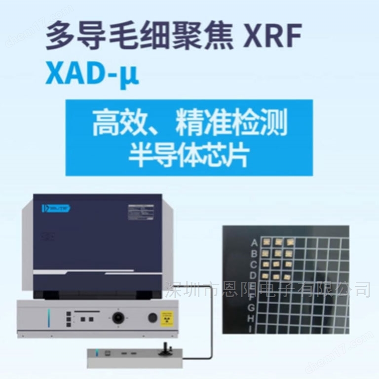


Energy dispersive X-ray fluorescence spectrometer with multi-channel capillary focusing XRF
NegotiableUpdate on 05/14
- Model
- Nature of the Manufacturer
- Producers
- Product Category
- Place of Origin
Overview
The XAD - μ - wafer energy dispersive X-ray fluorescence spectrometer with multi-channel capillary focusing XRF is a specialized instrument for analyzing and measuring ultra small measurement points or extremely thin coatings. It demonstrates advantages in automatic testing and analysis of coating thickness and composition in flexible circuit boards, chip packaging processes, and wafer micro areas. It can measure ultra small areas of microelectronic devices, advanced circuit boards, connectors, lead frames, and chips.
Product Details


Energy dispersive X-ray fluorescence spectrometer with multi-channel capillary focusing XRFIt is a specialized instrument for analyzing and measuring ultra small measurement points or extremely thin coatings, which demonstrates advantages in automatic testing and analysis of coating thickness and composition in flexible circuit boards, chip packaging processes, and wafer micro areas.
It can measure ultra small areas of microelectronic devices, advanced circuit boards, connectors, lead frames, and chips.
1)Equipped with micro focus enhanced typeX-ray generator and multi-channel capillary technology, capable of measuring diameters as small as 10 μ m
2)panorama+Micro area dual camera design provides a more comprehensive observation of samples, with resolutions as small as micrometers in the micro area, enabling faster and more convenient testing
3)based onThe new generation of film thickness measurement software EFP-T for EFP algorithm supports quantitative analysis based on standard samples and qualitative analysis without standard samples. It can simultaneously analyze 23 coatings and 24 elements
4)Large area high-resolutionDpp+Fast SDD detector, superior to 125eV
5)Measurement element range: AluminumAl(13)-铀U(92)
6)Scope of Coating Analysis: LithiumLi(3)-铀U(92)
7)Safety interlock, anti pinch andZ-axis anti-collision setting, V-zone laser protection, protecting the measuring head while measuring distance, wider range of measurable sample types
Equipped with a fully automatic programmable mobile platform, it can achieve unmanned operation and perform fully automatic testing on hundreds or thousands of samples

Industry applications:Bumping (Solder Bump Ag Content Detection)
Flip Chip is the largest market for excellent packaging, and bumping is its main process, significantly improving integration density. At present, top wafer manufacturers are pushing Bump Pitch to below 10 μ m, while domestic large packaging factories are approaching 40 μ m.
Bumping/μ-Bumping, (Micro) bump manufacturing technology is the fundamental engineering for the development and evolution of flip chip technology, and has evolved into packaging structures and processes such as TSV, WLP, 2.5D/3D, MEMS, etc. It is widely used in integrated circuit applications such as 5G, artificial intelligence, cloud computing, wearable electronics, IoT, big data processing and storage.
In the tin silver bump process, lead-free solder: tin silverSn-Ag, Tin silver copper Sn Ag Cu is widely used as lead-free solder on PCBs and Bumps. The concentration of silver in lead free solder bumps directly affects the melting point and quality of the solder, so the concentration requirements for silver content in solder quality management are very strict. However, the area of the convex block is very small, and under the low light flux of the conventional XRF small sample small collimator, it is difficult to accurately analyze the Ag content in it, making it difficult to achieve real-time optimization of the product process.
Industry application: Metal film deposition thickness and composition detection (PVD/CVD)
A chip is composed of a series of active and passive circuit components stacked together3D structure and thin film deposition are one of the core processes in chip front-end manufacturing. From the cross-section of the chip, it can be seen that the chip is composed of stacked layers of nanoscale components, with all active circuit components (such as transistors, storage units, etc.) concentrated at the bottom of the chip. The remaining part is composed of metal layers formed by aluminum/copper interconnects in the upper layer and insulating dielectric layers between each metal layer.
The preparation of thin films requires different technical principles, which leads to different technical principles and physical requirements for thin film deposition equipment/Chemical and other sedimentary methods complement each other.
The thin film deposition process is mainly divided into two categories: physical and chemical methods:
1) Physical method: refers to the use of physical processes such as thermal evaporation or sputtering of surface atoms of a substance under particle bombardment to achieve the transfer of substance atoms from the source substance to the surface of the substrate material. Physical methods include Physical Vapor Deposition (PVD), spin coating, Electrodeposition/Electroplating (ECD/ECP), etc
2) Chemical method: Steam containing gaseous or liquid reactants that make up the thin film elements is introduced into the process chamber with a reasonable gas flow, and a chemical reaction occurs on the substrate surface to deposit a thin film on the substrate surface. Chemical methods include Chemical Vapor Deposition (CVD) and Epitaxy (EPI), among others,
PVD is mainly used for depositing metal and metal compound thin films, and is mainly used for metal interconnect seed layers, barrier layers, hard masks, solder pads, etc. Magnetron sputtering PVD is mainly used for Al metal seed layer and TiN metal hard mask. Magnetron DCPVD in magnetron sputtering PVD is a widely used deposition method, especially for the deposition of planar thin films, such as metal layers of Al interconnects. However, its application in Cu interconnects (CuBs) has decreased, and TiN hard masks below 32nm have opened up new applications for this technology. Ionized PVD is mainly used as a barrier layer for Al, barrier layer and seed layer in CuBs, and can also be combined with metal CVD to deposit Ti adhesion layer in tungsten plugs.
CVD is commonly used for depositing insulating dielectric thin films, including gate oxide layers, sidewalls, barrier layers, PMD, and IMD, Barc, barrier layers, passivation layers, and other fields in the front and back stages. In addition, CVD can also prepare metal thin films (such as W).
XAD - μ - wafer is equipped with a domestically developed multi-channel capillary optical system, which can provide light spots as small as 10 μ m and thousands of times the intensity gain, and can solve the problems of AuAg、Al、Accurate testing of Ti/TiN, V, Ni, W, Cu, Mo coatings, with a conventional metal thin film thickness detection limit of up to 1nm.


Screenshot of EFP software operation interface:
1. Clear operation interface layout
The minimalist layout design allows operators to quickly master the basic software operations.
2. Design of Shortcut Button for Programs
Added shortcut key design buttons for daily plating programs, allowing for quick detection without the need to enter the program library and improve work efficiency.
3. High definition panoramic micro area visualization window
Users can clearly and intuitively observe the status of the tested sample by adjusting the zoom knobIdeal observation effect.
4. Real time monitoring data summary of instrument data
All data from the instrument can be observed at a glance, and any abnormalities will be immediately alerted by the system, greatly reducing operational errors.

| Product Name | Energy dispersive X-ray fluorescence spectrometer with multi-channel capillary focusing XRF |
| Product model | XAD-μ-wafer |
| Measurement element range | Al(13)- U(92) |
| Scope of Coating Analysis | Li(3)- U(92) |
| EFP algorithm | standard configuration |
| analysis software | Simultaneously analyze23 coatings, 24 elements |
| Same for different layers Element detection capability | standard configuration |
| software operation | Based on the new generationEFP algorithm, user-friendly closed software, automatic fault diagnosis, prompt correction, and operation steps to avoid misoperation |
| X-ray equipment | Micro focused enhanced radiation tube, with optional target materials:Mo、Rh、Cr、W |
| detector | DPP+Fast SDDdetector70mm² |
| Capillary focusing optical device | standard configuration15 μ m FWHM (optional 5-100 μ m) |
| optical filter | 8 types of filter switching devices |
| magnification | wide-angle+Micro area camera (optical magnification 330 times, digital magnification 1-6 times) |
| Z-axis movement range | Customized according to the sample, suitable for the itinerary>100mm |
| Sample table movement method | Fully automatic high-precisionXY platform |
| Sample table itinerary | 300 * 300mm (customizable to 600 * 600mm) |
| Other attachments | A set of computer, printer, accessory box, twelve element wafer (optional customized wafer transporter, edge finder, vacuum adsorption device, etc.) |
| X-ray standard | DIN ISO 3497, DIN 50987, and ASTM B 568 |
Similar Product Recommend


