- Phone
-
Address
Room 1301, Building A, Runchuang Building, No. 520 Chuangye 2nd Road, Bao'an District 70, Shenzhen
Product Categories
Shenzhen Tianye Instrument Co., Ltd
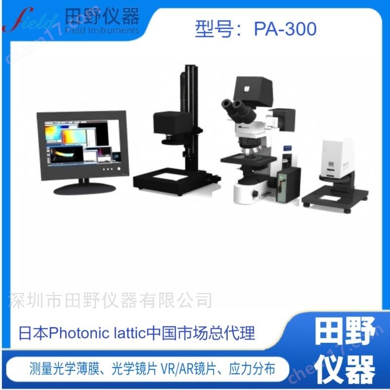


PHL residual stress measuring instrument
NegotiableUpdate on 05/06
- Model
- Nature of the Manufacturer
- Producers
- Product Category
- Place of Origin
Overview
The PA-300 series is a birefringence/stress measuring instrument developed by the Japanese company Photonic Lattice. The PA series measures birefringence within a range of 0-130nm and can measure samples ranging from a few millimeters to nearly 500 millimeters. The PA series birefringence measuring instrument, with its technology of photonic crystal polarizing array and birefringence algorithm design and manufacturing, has the ability to measure each sample in just a few seconds, making it the choice for birefringence measurement/stress measurement in the industry, especially in the industrial sector. PHL residual stress measuring instrument
Product Details
PHL residual stress measuring instrument
1、 Adaptation of core technology for substrate testing
1. Low phase difference precise capture technology
In response to the ultra-low phase difference requirement of quartz glass substrates (especially photomask substrates) ≤ 5nm, PA-3000.001nm minimum resolutionThe photonic crystal array detection unit, combined with the birefringence enhancement algorithm in the 520nm green light band, can capture the phase difference gradient changes between the substrate edge and the central area, and the detection sensitivity is three times higher than traditional polarized light interferometry. Its Stokes component synchronous acquisition technology avoids vibration errors caused by mechanical rotating components, ensuring stable repeatability accuracy of 12 inch substrate full area detection within σ<0.1nm. General agent for semiconductor quartz glass phase difference detector
2. Exclusive intelligent digital display system for substrate
• Partition digital imagingPA View software supports customized zone detection of substrates based on "effective area/edge area/positioning mark area", generating real-time color phase difference thermal maps. The red warning area can accurately lock stress concentration points (such as near substrate cutting marks), with a refresh rate of 3 seconds per time to meet the production line's requirements for intermittent shooting.
• Analysis of stress phase difference linkageAfter selecting the stress conversion module, the phase difference data can be directly converted into residual stress values at the MPa level, strictly matching the requirement of "residual stress ≤ 50MPa on spectral pure quartz substrate" in the ASTME837 standard. The data can be exported to the LIMS system of semiconductor factories with one click.
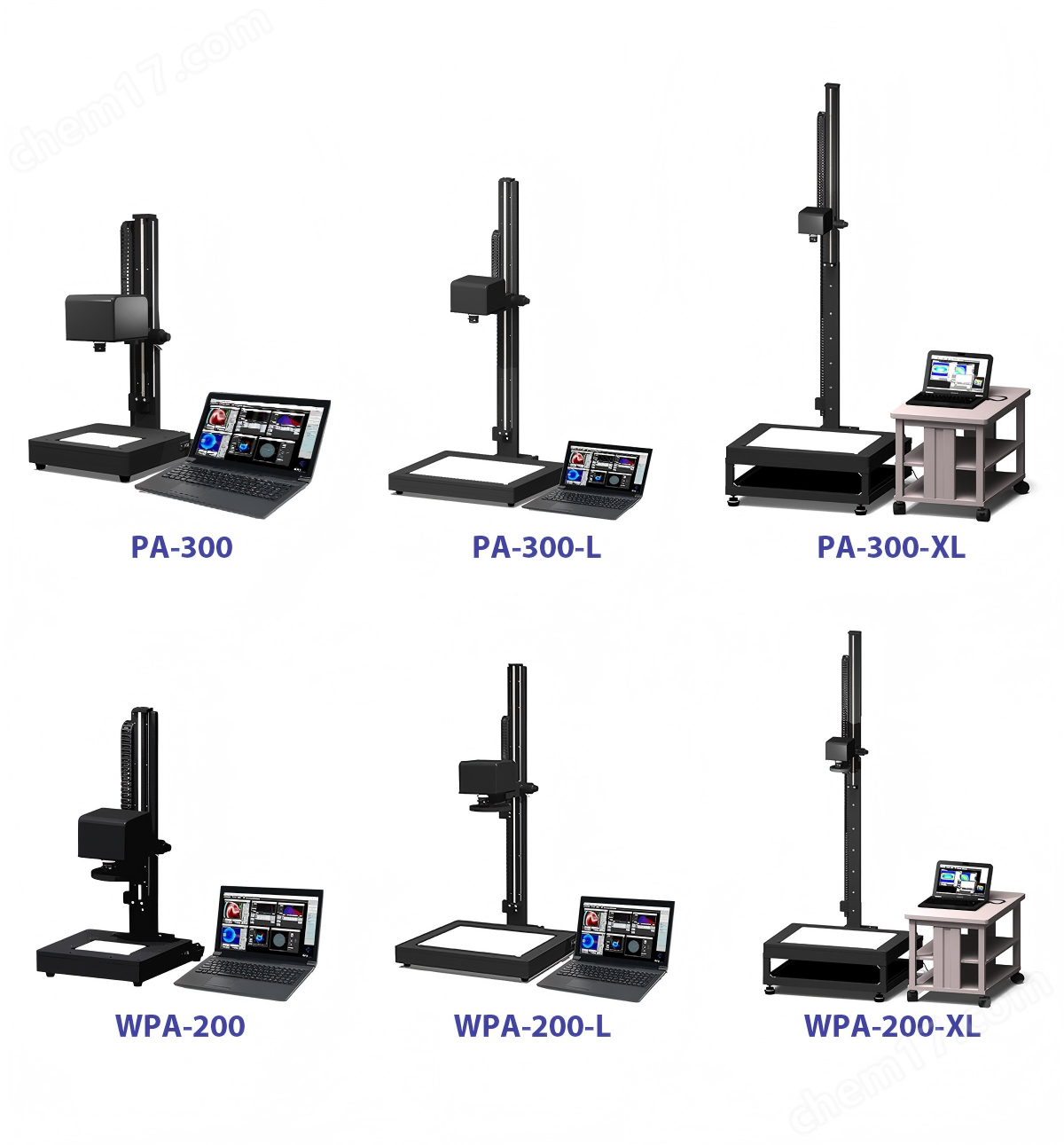
• Multi size adaptive calibrationFor 300mm wafer level substrates, the PA-300-XL model undergoes a single coverage inspection with a 242 × 290mm ultra large field of view, combined with an automatic splicing algorithm to eliminate the splicing errors of traditional segmented detection; For a 20 × 20mm small photomask substrate, a 7 × 8.4mm microscope lens can be selected to achieve micrometer level detail detection. Low phase difference detector
2、 The entire process of substrate testing conforms to the standard
1. Dual compliance with international/national standards
Test Items |
execution standard |
PA-300 implementation capability |
Residual stress detection |
SEMI F40 / GB/T 16523 |
0-130nm phase difference 0-200MPa stress conversion |
Phase difference uniformity |
SEMI P492 |
Global uniformity determination with σ<0.5nm |
Surface stress gradient |
ASTME837 |
Quantifying gradient changes in color mapping |
2. Cleanroom adaptation design
The equipment adopts an oil-free optical system and a dust-proof sealing structure, which meets the cleanliness level requirements of ISO 14644-1 Class 5 and can be directly deployed in the semiconductor front-end testing area. The GigE interface supports long-distance data transmission (up to 100 meters) to avoid interference from detection equipment on cleanroom airflow.
3、 Typical substrate inspection application scenarios
1. Semiconductor photomask substrate inspection
• test object6-12 inch circular quartz photomask substrate
• Core requirementsPhase difference uniformity ≤ 3nm, edge stress ≤ 30MPa
• PA-300 SolutionUsing PA-300-L type with vacuum adsorption sample stage, it automatically shields the substrate surface from dust interference; By using the built-in "photomask standard template" in the software, a detection report containing "phase difference mean/peak/uniformity" can be generated with just one click, directly connecting to SEMICON West certification requirements.
2. Inspection of smartphone cover substrate
• test object0.7-2mm ultra-thin quartz cover plate substrate
• Core requirementsQuickly locate local stress concentration caused by hot pressing molding
• PA-300 SolutionEnable the "Quick Scan Mode" to complete single substrate inspection in 3 seconds. With the automatic comparison function, it can simultaneously display the stress distribution heatmap of 10 substrates, helping process personnel quickly optimize annealing parameters and reduce defect rates by more than 40%.
4、 Summary of Core Advantages of Substrate Testing
1. Standard precise matchingThe testing process conforms to the dual standards of SEMI and GB/T, and the data can be directly used for international supply chain quality certification;
2. Intelligent digital display improves efficiencyPartition detection+automatic warning+data linkage, compressing substrate detection from "full inspection time of 3 minutes/piece" to "3 seconds/piece";
3. Full size coverageFrom 5mm miniature substrates to 50cm wafer level substrates, detection is achieved through a combination of lenses and machine models.
PHL residual stress measuring instrument
Similar Product Recommend


