-
E-mail
qgao@buybm.com
-
Phone
18117546256
-
Address
5th Floor, C7 Area, Chuangyan Intelligent Manufacturing, Lane 456, Dieqiao Road, Pudong New Area, Shanghai
Product Categories
Shanghai Boming Scientific Instrument Co., Ltd

Klar Mini Pro Microscope
NegotiableUpdate on 01/21
- Model
- Nature of the Manufacturer
- Producers
- Product Category
- Place of Origin
Overview
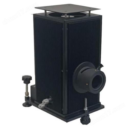
The Klar Mini Pro microscope is a compact and cost-effective microscopic spectroscopy and photocurrent module. High spatial resolution, specifically designed for researchers who have strict requirements for micro area research of materials.
Product Details
Mini Pro can generate mapping spectra of fluorescence and Raman by focusing the laser on the sample and collecting the emitted light (fluorescence or Raman) using a spectrometer. Automatic focusing can be achieved in the Z direction. The analysis software can quickly determine the peak energy and intensity of each spectrum. Obtain Mapping images with excellent resolution and contrast. Modular design enables researchers to quickly change wavelength ranges and experimental settings. The system can also be easily configured to obtain polarization spectra and reflectance spectra. It can also be combined with the probe station source table for photocurrent related testing
Appearance and Features


Features:
Laser excitation: 266-980 nm
Spectral range: 200-1700 nm
● Spatial resolution: μ m level
Can collect millions of spectra
● Fast peak fitting software
● Small and compact
Dark box design is protected from temperature changes, dust, and light
● High cost-effectiveness
Features: Laser can be quickly replaced

Interchangeable lasers: 266, 349, 375, 405, 532, 635, 785, 975. Acceptable customization of other lasers
Replacing the laser and related optical paths only takes a few minutes
versatile

Can be achieved:
PL (photoluminescence)
Raman
Mapping Scan
electroluminescence
Low temperature test
photocurrent
Powerful software fitting function

Z-axis automatic focusing

Optical path diagram and basic parameters


Typical configuration


Typical applications:
·Defect recognition in light-emitting diodes
·PL imaging of wide bandgap semiconductors
·Analysis of luminescent properties of two-dimensional materials
·Composition analysis of semiconductor alloys
·Fault Analysis and Quality Control
·Photoelectric current
The PL spectrum of green LED displays the intensity and peak energy of defect emission


Peak analysis can reveal characteristics such as composition. This figure shows the variation of high spatial resolution zinc content in cadmium zinc telluride materials.
High spatial resolution

High spatial resolution

(a) Raman spectra of titanium dioxide, including regions of rutile, rutile, and amorphous phases. (b) Raman spectra of the selected region. From "Localized phase transition of TiO2 thin films induced by sub bandgap laser irradiation," J. Vac. Sci. Tech. A (2021)

Photoelectric current D *, linearity, frequency range, and responsivity testing of ZnI2 and AgI
Similar Product Recommend