-
E-mail
mengxuehou@bmftec.cn
-
Phone
15261868162
-
Address
5th Floor, Building 26, Commercial Zone 6979, Hongshan Subway Station, Longhua District, Shenzhen, Guangdong Province
Product Categories
- Micro nano metal 3D printing system
- Industrial grade 3D printing
- Biological 3D printing
- Photosensitive resin material
- Micro nano 3D printing
- Post curing equipment
- PDMS mold flipping
- Multi material photopolymerization printing
- Multi material photopolymerization 3D printing
- Desktop level 3D printing
- Aluminum oxide ceramic 3D printing
Shenzhen Mofang New Materials Technology Co., Ltd

High precision photopolymerization 3D printer
NegotiableUpdate on 01/19
- Model
- Nature of the Manufacturer
- Producers
- Product Category
- Place of Origin
Overview
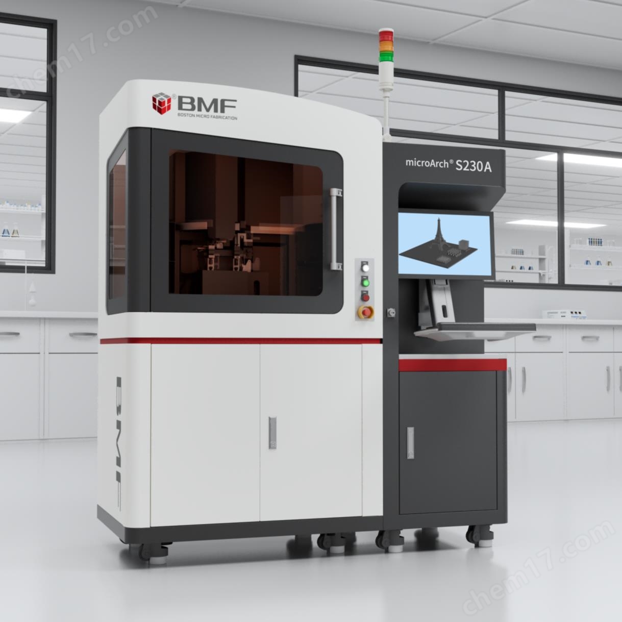
Mofang high-precision photopolymerization 3D printer microArch; S230 (accuracy: 2 μ m), constructed based on surface projection micro stereolithography technology (P μ SL). Fully automatic horizontal adjustment system: three major systems including platform automatic leveling, film surface automatic leveling, and rolling cutter automatic adjustment, which improves printing efficiency by nearly 50 times.
Product Details
Mofang PrecisionHigh precision photopolymerization 3D printermicroArch ® S230A, Relying on innovative P μ SL technology, it achieves optical accuracy of up to 2 microns and supports printing with photosensitive resin and ceramic paste. This technology is based on digital light processing (DLP) systems, which project ultraviolet light onto the surface of photosensitive materials to precisely cure each layer of microstructure. Compared to traditional point scanning methods, P μ SL uses full layer exposure, which results in faster printing speed, higher structural consistency, and better edge clarity.
1 microArch ® S230A device specifications
Light source: UV-LED (405nm)
Printing materials: photosensitive resin, ceramic paste
Optical accuracy: 2 μ m
Printing layer thickness: 5-20 μ m
Print sample size:
Mode 1: Single Projection Mode: 3.84mm (L) × 2.16mm (W) × 50mm (H)
Mode 2: Splicing mode: 50mm (L) × 50mm (W) × 50mm (H)
Mode 3: Repeat Array Mode: 50mm (L) × 50mm (W) × 50mm (H)
Print file format: STL
System dimensions: 1720mm (L) × 750mm (W) × 1820mm (H)
Weight: 660kg
Electrical requirements: 220~240V AC, 50/60HZ, 2KW
Equipment Characteristics and Advantages
Ultra high precision: optical accuracy up to 2 μ m;
Configure laser ranging for easy leveling of printing platforms and release films;
Configure rolling cutters for fast leveling of printing materials and support printing of high viscosity resins;
Equipped with a high-precision motion control system, the repeated positioning accuracy of XYZ motion axes is ± 0.2 μ m;
Industrial grade equipment standards, easy to operate and maintain;
Configure air flotation platform to improve printing quality;
Excellent stability of light source;
Customized printing software and slicing software.
IImicroArch® S230AApplication field
1. Microfluidic chip manufacturing
In fields such as life sciences and POCT (point of care diagnostics), the channel width of microfluidic chips often ranges from tens of micrometers to even smaller. The Mofang 2 μ m micro nano 3D printing equipment can be applied to the construction of microfluidic platforms, organ chips, and single-cell analysis platforms. Its high-precision printing capability effectively ensures channel size consistency and liquid transfer efficiency, assisting in the precise integration of biomedical microsystems.
2. Precision optical structure and micro lens array
Traditional microlenses or free-form surface components rely heavily on ultra precision CNC or injection molding, resulting in high costs and long development cycles. With the help of 2-micron precision 3D printing technology, users can quickly design and manufacture high curvature free-form surface optical structures for enhancing optical performance in fields such as VR/AR imaging, terahertz waveguides, and optical waveguide communication.
3. Micro devices and sensors
In the fields of sensors, microactuators, etc., Mofang Precision supports in situ manufacturing of micrometer level connection channels and complex structures, providing a solution path for the research and development of miniaturized and integrated electronic components. Meanwhile, the compatibility of materials such as ceramics and photosensitive resins also enables these devices to have stronger environmental adaptability.
Similar Product Recommend


