-
E-mail
li.fu@perkinelmer.com
- Phone
-
Address
1670 Zhangheng Road, Zhangjiang High tech Park, Shanghai
PerkinElmer Enterprise Management (Shanghai) Co., Ltd
PerkinElmer appeared at the second "Semiconductor Materials and Device Measurement and Testing Technology Training Course"
Date: 2025-10-31Read: 0
NEWS
”
From October 28th to 30th, 2025, byShanghai Institute of Silicate, Chinese Academy of SciencesHosted byThe Second Training Course on Measurement and Testing Technology for Semiconductor Materials and DevicesSuccessfully held in Shanghai. As a leading global provider of analytical instruments and solutions,PerkinElmer invited to exhibit and deliver a special report, comprehensive displayIn the field of semiconductor material testingOur cutting-edge technology and localized service capabilities.

Meeting Background
semiconductorThe industry is technology intensive and complex, involving hundreds of precision processes. As the manufacturing process continues to shrink, the purity of materials, manufacturing accuracy, and quality control are also growing exponentially. In order to strengthen the construction of a high skilled talent team and enhance the understanding and application ability of scientific researchers towards advanced analytical technologies, this training course brings together86 professional students from research institutes, universities, and enterprises/institutionsSurroundingHot topics such as optoelectronic materials, third-generation semiconductor materials, sensors and MEMS, reliability testing, failure analysis, defect detection and measurementExpand system training.
Perkin Elmer made a brilliant appearance
We have set up a professional booth on site to showcase our full process analysis and testing solutions for the semiconductor industry, covering:
High purity material impurity analysis (ICP-MS)
Trace element detection (AAS, ICP-OES)
Material structure and composition characterization (UV, IR, TEA)
Analysis and detection of organic pollutants and chlorosilanes (GC/MS)
Attract numerous researchers to stop and exchange ideas, and deeply explore the practical application challenges in precursor, wafer, packaging and other processes.

Speaker: Zhu Min
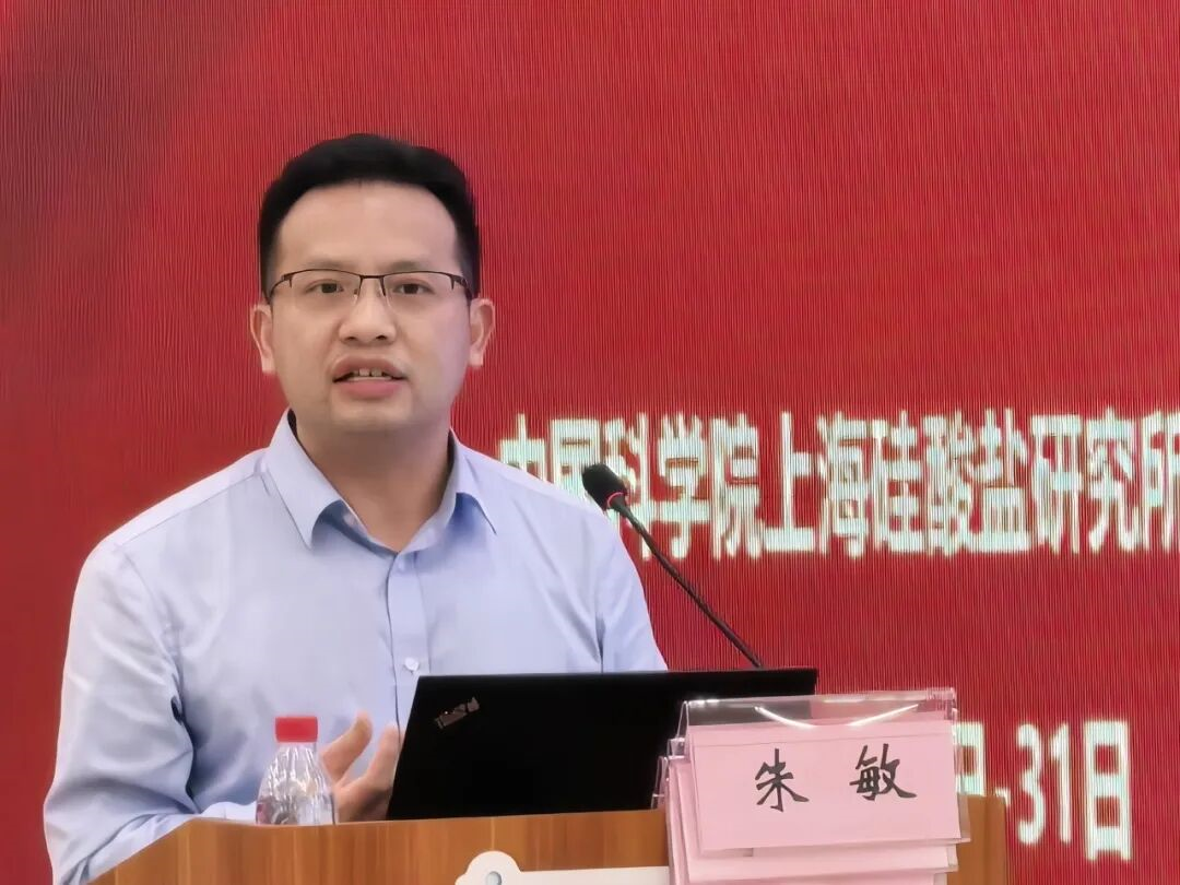
?PerkinElmer Analytical Instruments Application Technology Manager

Summary of Report Content
The reporting system has been introducedApplication of ICP-MS technology in the detection of semiconductor metal based materials, with a focus on analyzing the key challenges faced by the analysis, such asMatrix effects, mass spectrometry interference, and stability of instruments for long-term analysis, etcTo address these challenges, he introduced relevant solutions and optimization methods, such as full substrate gas dilution technology, plasma condition selection, universal pool anti-interference parameters, and the excellent performance of advanced three cone large aperture interface and quadrupole ion deflection technology in substrate tolerance and space charge effect. He also focused on the application cases and experimental data of precursors.
Finally, he emphasized,technological innovationandWhole process quality controlIt is to promote the development of semiconductor materialsHigher purity and consistency developmentThe key,PerkinElmer will rely on comprehensive professional service capabilities and Shanghai Zhangjiang Semiconductor Cleanroom,Continuously delve into the forefront of analytical technologyTo provide solid technical support for industry progress and customers.
Follow us


