-
E-mail
info@giantforce.cn
-
Phone
18911365393
-
Address
1311, Building B, Wanda Plaza, No. 58 Xinhua West Street, Tongzhou District, Beijing
Juli Optoelectronics (Beijing) Technology Co., Ltd
Deep analysis of Voc (open circuit voltage) loss mechanism in perovskite solar cells
Date: 2025-09-10Read: 44
Perovskite solar cells (PSCs) have become a research hotspot in the field of photovoltaics due to their high photoelectric conversion efficiency (PCE) and low-cost preparation advantages. However,Open circuit voltage (Voc) lossIt is one of the core bottlenecks that restricts its efficiency from approaching the theoretical limit. Voc loss refers to the actual Voc of a battery and the "Shockley Queisser (S-Q) limit Voc" (based on material bandgap theory)upper limitUnderstanding the source and mechanism of the difference in Voc is crucial for optimizing battery performance.
1、 Theoretical basis of Voc loss: from S-Q limit to actual value
To understand Voc loss, it is necessary to first clarify the difference between "theoretical Voc" and "actual Voc":
·S-Q limit VocBased on the ideal PN junction model, determined solely by the material bandgap (Eg), temperature (T), and solar spectrum, the formula is:

among which,JscTo measure the short-circuit current density,J‘0The actual dark saturation current density is significantly increased due to non ideal factors such as carrier recombination and interface potential barriers.
The essence of Voc loss: Caused by non ideal factorsJ‘0Far greater than idealJ0Or the separation/transport efficiency of photo generated charge carriers may decrease, ultimately resulting in actual Voc below the S-Q limit.
2、 The core source and mechanism of Voc loss
Based on the "physical location" and "functional link" where the loss occurs, Voc loss can be divided intoIntrinsic loss(Caused by the perovskite body) andNon intrinsic loss(Caused by interface, defects, and carrier transport layer), the specific mechanism is as follows:
(1) Intrinsic loss: the inherent characteristics of perovskite body
The intrinsic loss is determined by the electronic structure and carrier dynamics of the perovskite material itself, and cannot be determinedallThe eliminated 'basic losses' mainly include the following two types:
1. Bandgap Voc intrinsic offset (non radiative recombination "* low limit")
In an ideal situation, Voc should be close to the voltage corresponding to the bandgap (Eg/q, such as FAPbI)₃Eg/q ≈ 1.48 V), but even without defectsexcellentPerovskite and Voc can also be affected byInherent non radiative recombinationBelow Eg/q:
· Physical essence: The valence band top (VBM) and conduction band bottom (CBM) of perovskite have "Urbach tails", which originate from lattice vibrations (phonons) or electron electron interactions, allowing charge carriers to undergo non radiative recombination through "sub bandgap transitions" (such as electrons transitioning from CBM to tail states near VBM, and then releasing energy through phonons).
· Loss amplitude: This type of inherent loss is usually0.1~0.2 VThe perovskite with Eg=1.5 eV has an intrinsic lower Voc limit of approximately 1.3-1.4 V, which is the source of the difference between the S-Q limit Voc and Eg/q.
2. Non radiative recombination of charge carriers (dominated by intrinsic defects)
In the perovskite bodyIntrinsic defect(such as vacancies and interstitial atoms) will form "recombination centers", accelerating the non radiative recombination of photo generated carriers, directly leading to a decrease in Voc:
Typical defect types:
· iodine vacancyVI+In lead iodide (FAPbI)₃)Or cesium lead iodide (FACsPbI)₃)It is common to form shallow level defects, which have weak carrier trapping ability but can prolong the recombination lifetime and indirectly reduce Voc;
· Lead vacancyVPb2-Or iodine interstitial atomsIi-Forming deep level defects that can efficiently capture electrons/holes (such as...)VPb2-)Capture voids,Ii-The capture of electrons, followed by non radiative deactivation through Shockley Read Hall (SRH) recombination, is the main contributor to the bulk Voc loss.
· Loss characteristics: The higher the density of defects in the body (usually referred to as "defect state density")Nt”The faster the non radiative recombination rate,J‘0The larger the Voc loss, the more significant it is (such as when the defect density increases from (10 ^ 15cm ^ -3) to 10 ^ 17cm ^ -3), and the Voc can decrease by 0.05~0.1 V).
(2) Non intrinsic losses: losses caused by interface and device structure
Non intrinsic losses arise from the interface between perovskite and the carrier transport layer (electron transport layer ETL, hole transport layer HTL), electrode contact, or defects within the transport layer itself, and are currently the core direction of optimization, accounting for over 60% of the total Voc losses.
1. Non radiative recombination at the interface of perovskite/transport layer (* main non intrinsic losses)
Perovskite and ETL (such as TiO)₂、SnO₂)The interface of HTL (such as Spiro OMeTAD, PTAA) is a key region for carrier separation, but it has also become a "disaster area" for non radiative recombination due to "energy level mismatch" and "interface defects":
(1) Composite caused by energy level mismatch
The ideal interface needs to meet the "energy level alignment" (such as the conduction band bottom of ETL being lower than that of perovskite CBM, and the valence band top of HTL being higher than that of perovskite VBM) to promote carrier separation; If the energy levels do not match, a "potential barrier" or "trap" will be formed:
· Case 1: ETL (such as TiO)₂)The conduction band bottom is too high (with a difference of less than 0.1 eV compared to perovskite CBM) → electrons are difficult to inject from perovskite into ETL, and the trapped electrons and holes recombine at the interface;
· Case 2: The valence band top of HTL (such as Spiro OMeTAD) is too low (with a difference of less than 0.1 eV compared to perovskite VBM) → it is difficult to inject holes into HTL, resulting in interface hole accumulation and electron recombination.
· Loss amplitude: Voc loss caused by energy level mismatch can reach up to0.05~0.15 V(such as TiO)₂/Due to energy level mismatch at the perovskite interface, Voc is higher than SnO₂/The interface of perovskite is 0.08~0.1 V lower.
(2) Composite caused by interface defects
There are numerous "dangling bonds," "lattice mismatch defects," or "chemisorbed impurities" (such as O) at the interface between perovskite and transport layer₂、H₂O), Forming deep level recombination centers:
· Typical defect: TiO₂Surface oxygen vacanciesVo2+It will capture electrons in perovskite and recombine with holes transported by HTL; Pb ² on the surface of perovskite⁺Unconjugated defects (dangling bonds) will capture holes and recombine with electrons in ETL.
· Loss characteristics: The non radiative recombination rate at the interface is much higher than that of the body (due to high interface carrier concentration and defect density), which is the main reason for the Voc loss of low efficiency PSCs (such as unmodified interface PSCs, Voc loss can reach 0.3-0.4 V).
· Loss amplitude: The Voc loss caused by the transport layer is usually 0.03~0.1 V (such as SnO)₂After doping optimization, the Voc of ETL can be increased by 0.05~0.08 V.
2. Loss of Carrier Transport Layer (ETL/HTL)
The poor conductivity and numerous defects of ETL or HTL can hinder the transport of charge carriers, indirectly reducing Voc
· Poor conductivity: If HTL (such as Spiro OMeTAD) has low hole mobility (<10)⁻⁴cm²/(V・s)), Holes will accumulate in HTL, leading to an increased probability of interface electron hole recombination;
· Self defects: ETL (such as SnO)₂)Sn ² in the middle⁺Defects can form electronic traps that capture electrons injected from perovskite, leading to a decrease in electron transport efficiency and Voc;
· Loss amplitude: The Voc loss caused by the transport layer is usually0.03~0.1 V(such as SnO)₂After doping optimization, the Voc of ETL can be increased by 0.05~0.08 V.
3. Electrode contact loss
Excessive contact resistance between metal electrodes (such as Au, Ag) and HTL, or direct contact between electrodes and perovskite (without transport layer), can lead to carrier recombination:
· Contact resistance: If the contact resistance between HTL and Au electrode is greater than 10 Ω・cm², Difficulty in injecting holes from HTL into the electrode leads to hole accumulation and increased recombination;
· Direct contact: The Fermi level of the metal electrode does not match the perovskite level, forming a "Schottky barrier" that hinders carrier transport. At the same time, metal atoms (such as Au) may diffuse into the perovskite to form defects, exacerbating recombination;
· Loss amplitude: Electrode contact loss is usually small(0.02~0.05 V)However, the preparation of inferior electrodes (such as high temperature during Au evaporation) will significantly increase losses.
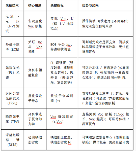
3、 Quantitative and characterization methods for Voc loss
Accurately quantifying and locating Voc losses is a prerequisite for optimization. Common characterization techniques can be divided into two categories: "macro loss quantification" and "micro mechanism analysis":
4、 Optimization strategy for Voc loss
Regarding the above-mentioned sources of losses, the current mainstream optimization direction focuses on "suppressing non radiative recombination" and "optimizing energy level alignment". The specific strategies are as follows:
1. Passivation of body defects: reducing intrinsic losses
· Cation doping: using Cs⁺、Rb⁺Partial replacement of FA⁺(such as FACsPbI)₃)Inhibit lattice distortion of perovskite and reduce VI+、VPb2-Defects;
· Anion doping: using Br⁻Partial replacement of I⁻(such as FAPbI)₂Br), Narrowing the Urbach tail width and reducing intrinsic non radiative recombination;
· Defect passivator: Adding guanidine salts (such as GuaI), thiourea, etc. to perovskite precursors through coordination interactions (such as N and Pb ²)⁺Combining passivation of surface/bulk defects.
2. Interface Engineering: Eliminating Non Intrinsic Core Losses
· Interface passivation: using Al₂O₃、 Inorganic layers such as LiF, or organic molecules such as PCBM and PEAI, modify the ETL/perovskite and perovskite/HTL interfaces to fill dangling bonds and inhibit defect recombination (such as PEAI modified perovskite surfaces, which can increase Voc by 0.1-0.15 V);
· Energy level regulation: through ETL doping (such as SnO)₂Doping W⁶⁺Lowering the conduction band bottom, HTL modification (such as PTAA doping with LiTFSI to enhance hole mobility), optimizing interface energy level alignment, and promoting carrier separation.
3. Transport layer optimization: improve carrier transport efficiency
· ETL optimization: using SnO₂Replace TiO₂(SnO₂Lower conduction band bottom for better energy level matching, or prepare dense, low defect ETL through ALD (atomic layer deposition);
· HTL optimization: Developing high mobility HTL (such as NiO)ₓInorganic HTL, migration rate>10⁻²cm²/(V・s)), Replace Spiro OMeTAD to reduce HTL defects and resistance.
4. Device structure innovation: reducing contact losses
· HTL free structure: using carbon electrodes to directly contact perovskite, avoiding HTL defects and cost issues;
· All inorganic structure: using CsPbI₃Perovskite+inorganic ETL/HTL (such as TiO)₂/NiOₓ)Improve stability while reducing interface recombination caused by organic layers.
5、 Summary and Challenge
The Voc loss of perovskite solar cells is the result of the combined action of "intrinsic characteristics" and "extrinsic device defects", among whichInterface non radiative recombinationandComposite of body defectsIt is currently the main source of loss. Through "defect passivation," "interface engineering," and "energy level optimization," the Voc of high PSCs has been increased from the early 0.9 V to over 1.2 V (based on perovskite with Eg ≈ 1.5 eV), but there is still room for optimization at 0.15~0.2 V from the S-Q limit.
Future challenges include:
1. How to further reduce "intrinsic non radiative losses" (such as narrowing the Urbach tail through quantum confinement effects);
2. Develop a long-term stable passivation layer to avoid passivation agent failure under light/humid conditions;
3. Realize uniform control of Voc loss in large-area devices (currently efficient devices are mostly small in size, with more interface defects and higher Voc loss in large areas).
A deep understanding of the Voc loss mechanism and targeted optimization is the key to breaking through the efficiency of perovskite cells by 30% (S-Q limit of about 33%).
