-
E-mail
qeservice@enli.com.tw
-
Phone
18512186724
-
Address
Room 409, Building A, No. 169 Shengxia Road, Pudong New Area, Shanghai
Guangyan Technology Co., Ltd
Single Point to Mapping: Analyzing Ten Top Journals and How QFLS Became a Core Tool for Photovoltaic Diagnosis
Date: 2025-10-23Read: 1
Preface
Quasi Fermi level splitting in solar photovoltaics and advanced materials research(QFLS)And its spatial distribution mapping(QFLS mapping)It is a key tool for understanding materials, diagnosing device bottlenecks, guiding new material development, and process optimization.
QFLSIt is the chemical potential difference between photo generated charge carriers (electrons and holes) in a non-equilibrium state. In theory, it is directly equal to the open circuit voltage of an ideal device(Voc). However, in actual devices, there is an electrochemical potential loss at the interface between the transport layer and the electrode, leading to this ideal relationship'mismatch'Analyzing this mismatch is the breakthrough point for improving photovoltaic technology.
QFLSWhy is it so important in photovoltaic research?
QFLSDirectly measuring the quality of the photovoltaic absorption layer material represents the theoretical upper limit of the device's open circuit voltage. We calibrate photoluminescence through calibration(PL)Direct measurement of spectraQFLSTo avoid complex interface issues during the production of complete devices. passQFLSIt can directly evaluate the composite activity of the material itself, helping researchers understand its inherent potential in the early stages of material development.
QFLSMeasure the direct quantification of radiative and non radiative recombination losses in solar cells. Non radiative recombination is causingQFLSThe main reason for deviating from the radiation limit. Through this difference, it is possible to accurately identify the root cause of voltage loss: whether it comes from the material itself or interface issues.
interpretationQFLSandVocof“The Mystery of Mismatch”
In theoryQFLSShould be equal to the external open circuit voltage of the deviceVoc(Voc = ΔEF/q). But in actual devices, there are often differences between the two. This difference reveals the existence of electrochemical potential loss at the interface.
GermanyFraunhofer ISEofUli WürfelThe professor's team is2021Year by year《Energy Technology》It is pointed out that planar perovskite solar cellsVocimproved250mVButPLThe signal changes less than twice[1]They believe that this can be achieved by using the quasi Fermi level of minority charge carriers(QFL)Explain the gradient towards the corresponding electrode direction. Carrier velocity saturation in heterojunctions may lead toQFLDiscontinuity. Under the influence of ion movement, the mismatch phenomenon is more pronounced. This indicates that even if the material itself has good quality, if the electrochemical potential transmission at the interface is poor, the externalVocIt also cannot reflect the internal situationQFLSThe potential.
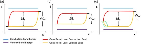
Image taken from:Ion Movement Explains Huge VOC Increase despite Almost Unchanged Internal Quasi-Fermi-Level Splitting in Planar Perovskite Solar Cells – Fig.2
GermanyPotsdam UniversityofMartin StolterfohtThe professor's team is2021Year by year《Advanced Energy Materials》In the middle, it elaborates in detailQFLS-VocMismatched mechanism[2]They defined the selectivity factor for most charge carriers(selectivity, Se,maj)This factor is related to the contact resistance between majority and minority charge carriers. Through the diagram1The band diagram shows how selective and non selective hole contact layers affect each otherQFLThe degree of curvature, which in turn leads toQFLS-VocNot matching. The presence of a low mobility intermediate layer can also lead to serious consequencesQFLS-VocNot matching, even thoughQFLSContinuously improving,VocBut it may decrease.Fig. 5(b)The5(c)and5(d)The simulation results show how the low mobility intermediate layer affectsQFLSThe gradient andVocThe downward trend.
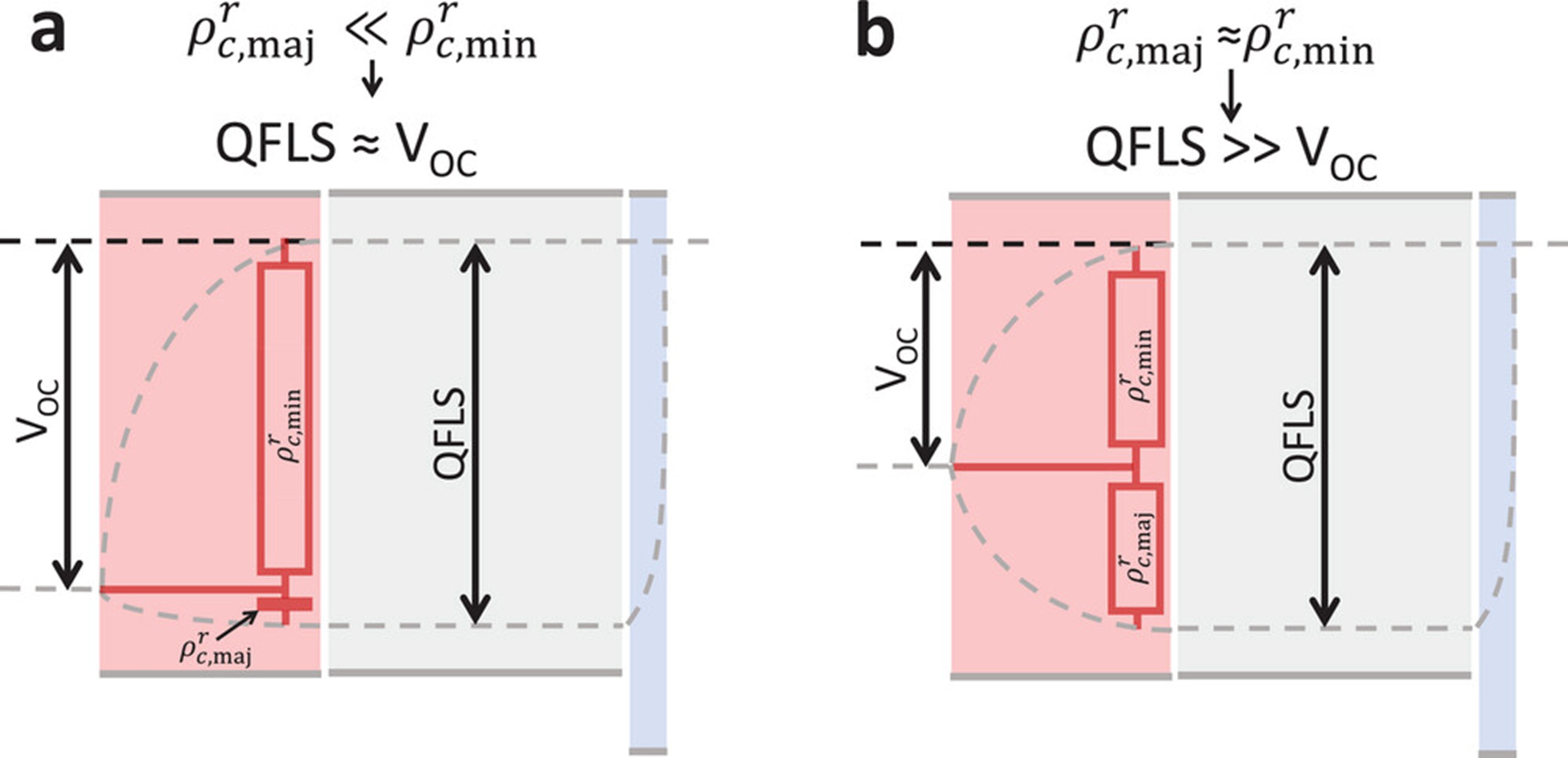
Image taken from:Mismatch of Quasi–Fermi Level Splitting and Voc in Perovskite Solar Cells – Fig.1
To quickly screen materials with high efficiency potential and optimize transport layer materials,QFLS-MaperTesting equipment can provide fast and accurateQFLSMeasure and predict the theoretical efficiency upper limit of the material, and generatePseudo J-VCurve. In this way, researchers can quickly grasp the material potential before component preparation, significantly reducing trial and error costs and time.
QFLS MappingVisualization reveals material uniformity and defects
single pointQFLSMeasurement is important, but the uniformity of materials at the microscale has a decisive impact on device performance.QFLS mappingTechnology can provide material surfacesQFLSVisualized images of distribution make the quality of materials clear at a glance. passQFLS mappingCan directly observe various areas of the materialQFLSDifferentiate, identify local defects or unevenness issues.
the United KingdomUniversity of CambridgeofSam StranksProfessor teamIn2025Year by year《ACS Energy Letters》Using hyperspectral absolutePLImaging technology has obtained data on secondary batteriesQFLSMapping diagram[3]They comparedGO/2PACzConnecting batteries in series with reference batteriesQFLSDistribution, results showGO/2PACzSeries connected batteries with low bandgap(LBG)And broadband gap(WBG)The secondary battery exhibits more uniform performanceQFLSDistribution. This indicates that non radiative recombination is suppressed and internal and external voltage losses are improved.Fig. 3(a)and3(b)ofQFLSImage, andSupplementary Fig. S14andS15ofQFLSDistribution histogram, visually displaying the relationship between different interface layersQFLSThe impact of uniformity.
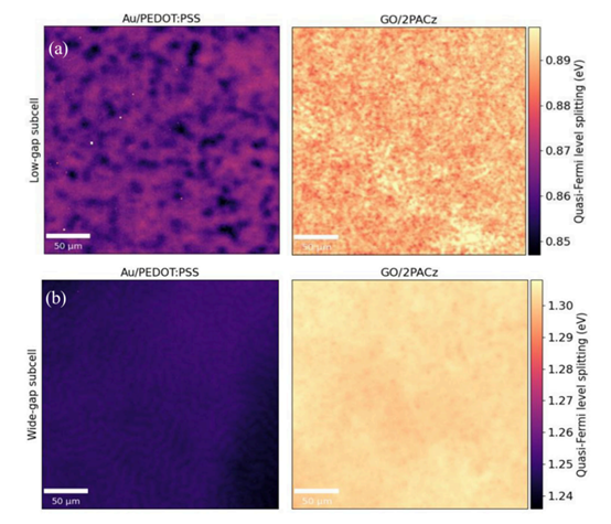
Image taken from:Optimized Graphene-Oxide-Based Interconnecting Layer in All-Perovskite Tandem Solar Cells – Fig.3ab
Professor Hou Yi's team from the National University of SingaporeYu2024Published in《Energy & Environmental Science》In the paper, the characteristics of different perovskite thin films were demonstratedQFLSImaging image[4]They found that afterPhAThe modified film shows higher performance in the entire detection areaQFLSValue and better spatial uniformity, which provesPhAIt can passivate defects, reduce non radiative recombination, and thus improve the optoelectronic quality of perovskite films.Fig. 3(a)These results are presented.

Image taken from:Surpassing 90% Shockley–Queisser VOC limit in 1.79 eV wide-bandgap perovskite solar cells using bromine-substituted self-assembled monolayers – Fig.3a
throughQFLS-MaperTesting equipment allows researchers to perform in just a short amount of time3Obtain within secondsQFLSVisualization diagram. This not only allows for a quick grasp of the overall material qualityQFLSThe distribution situation and real-time evaluation of material uniformity and defects have irreplaceable advantages for material screening and process monitoring in the early research and development stage.
Quantitative energy loss: fromPLQYtoQFLS
QFLSNot only can it qualitatively judge material quality, but it can also quantitatively analyze energy loss.QFLSThe calculation formula is:QFLS = kBT ln (PLQY × JG / J0,rad)Here'sPLQYIs the photoluminescence quantum yield,JGIs the photo generated current density,J0,radIt is the saturation current density of dark radiation. Through these parameters, the ratio of radiative and non radiative composite losses can be accurately decomposed.
GermanyPotsdam University Martin StolterfohtProfessor teamYu2020Published in《ACS Applied Materials & Interfaces》In the paper, utilizingPLQYandJGQuantified itQFLS [5]They found that by comparing the measurementsQFLSRegarding the radiation limitVOC,MAPIThere is non radiative recombination loss in both the perovskite film and the three cation perovskite film(MAPIabout200 meVThree cation perovskite is approximately110 meV). They also observed thatHTL/Perovskite interface and perovskite/C60The composite loss of the interface increases.Table 2Listed the data for these losses,Supplementary Fig. S5Showing these losses. This study demonstrates thatQFLSHow to accurately locate composite hotspots.

Image taken from:Defect and Interface Recombination Limited Quasi-Fermi-Level Splitting and Open-Circuit Voltage in Mono – Fig.2
Professor Pang Shuping from the Chinese Academy of Sciences Qingdao Institute of Bioenergy and ProcessIn2024Year by year《Advanced Materials》In the middle, utilizingQFLSQuantify the energy loss caused by non radiative recombination in perovskite solar cells[6]They utilizeEQESpectral calculationJG, combined with blackbody radiation spectrum calculationJ0Accurate evaluationQFLS.
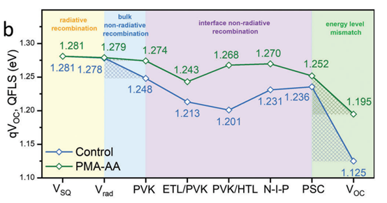
Image taken from:Enhanced Quasi‐Fermi Level Splitting of Perovskite Solar Cells by Universal Dual‐Functional Polymer – Fig.4b
Professor Li Gang's team from The Hong Kong Polytechnic UniversityYu2025Year by year《Advanced Materials》In the middle, usingQFLS = qVoc,rad + kBT ln(PLQY)Low formula analysisVOCThe source of losses[7]They found thatSnO2/At the buried interface of perovskite, energy loss is achieved through its strategyΔ(VOC,rad−QFLS)from62 meVreduce to34 meV.Fig. 4(e)andTable S5Presented these data, confirming ultra-lowVOCThe loss is mainly attributed to the elimination of non radiative recombination at the interface.
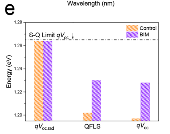
Image taken from:Buried Interface Regulation with a Supramolecular Assembled Template Enables High-Performance Perovskite Solar Cells for Minimizing the VOC Deficit – Fig.4e
QFLS-MaperThe detection equipment relies on its high6An order of magnitudePLQYSensitivity, able to measure from1E-4%ofPLQYMeasure the value. Moreover, it adoptsNISTTraceable components and internationally recognized measurement methods ensureQFLSAccuracy of measurement. This enables researchers to accurately quantify non radiative recombination losses, providing reliable data support for material optimization.
Guide to Materials and Interface Engineering
QFLSNot only a diagnostic tool, but also a guide for materials and interface engineering. passQFLSIt can evaluate the effect of different transport layer materials and the influence of chemical cleaning or annealing processes on the surface properties of the absorption layer.
LuxembourgUniversity of Luxembourg Susanne SiebentrittProfessor teamYu2018Published in《IEEE Journal of Photovoltaics》In the paper, we discussedNaFandNaF+RbFPost sedimentation treatmentCIGSThe influence of thin films[8]They found that afterNaF+RbFThe processed absorption layer,QFLSHigher than just passing throughNaFThe processed samples are attributed to a reduction in non radiative recombination, even inCdSIt occurred before sedimentation. Even if the absorption layer is exposed to air and undergoes surface degradation, after being treated with heavy alkali metals, itQFLSThe same upward trend is also observed, indicating that alkali metal treatment improves the quality and surface of the absorption layer itself.Fig. 3These trends are presented.

Image taken from:Influence of Sodium and Rubidium Postdeposition Treatment on the Quasi-Fermi Level Splitting of Cu(In,Ga)Se2 Thin Films – Fig.3
AlgeriaHigher National School of Renewable EnergiesofHichem BencherifProfessor teamYu2025Year by year《Solar Energy》In the middle, research has been conducted on3DIntroduction into perovskite2DThe influence of double junction layers and different hole transport layers[9]They found that these optimizations improvedPLQYandQFLSThis indicates a reduction in non radiative losses.Fig. 5andTable 6Showcased the effects of these improvements.

Image taken from:Achieving Quasi-Fermi level splitting near its radiative limit in efficient and stable 2D/3D perovskite solar Cells: Detailed balance model – Fig.5a
QFLS-MaperThe detection equipment can perform rapid layeringQFLSTest and support in-situ time phase changesPLanalyze Researchers can evaluate the impact of each material on overall performance layer by layer during the preparation process, quickly identify bottlenecks, and optimize process conditions and material selection.
In depth exploration of carrier dynamics and defect control
QFLSIt is not only related to the macroscopic device performance, but also deeply reflects the microscopic carrier concentration, lifetime, and doping level. higherQFLSThis may indicate lower composite activity or higher doping concentration. To accurately distinguish between these two effects, it is necessaryQFLSCombining with other measurement methods.
Professor Du Zuliang's team from Henan University in China2023Year by year《Nature Communications》In the discussion, we explored how to increaseQFLSTo reduce the heat generation of quantum dot light-emitting diodes[10]They found that for a given electron density, if the absorption rate of the film remains constant, it decreasesQDThe packing density can increase the electron densityQFLSAlthough this study focuses onLEDBut its core idea——Improving carrier management through optimizationQFLSThis also applies to the field of photovoltaics.
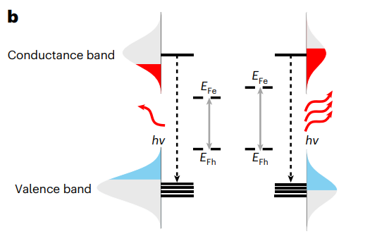
Image taken from:Minimizing heat generation in quantum dot light-emitting diodes by increasing quasi-Fermi-level splitting – Fig1b
QFLS-MaperTesting equipment can not only quickly obtainQFLSData, with its multimodal functionality, also allows for integration with other measurement techniques, such as time resolutionPL(TRPL)Thus, a more comprehensive analysis of deep physical mechanisms such as carrier lifetime, doping concentration, and defect density can be conducted.
Conclusion
QFLSAnd its mapping technology has become a tool for photovoltaic research. It not only provides a means to quantify energy loss, but also plays a guiding role in material screening, interface engineering, process optimization, and basic physics understanding. From macroscopic device performance diagnosis to microscopic carrier dynamics and defect control,QFLSProvided multidimensional insights and accelerated the development process of the new generation of high-efficiency photovoltaic devices. Master and make good use of itQFLSAnalysis is an important skill for any professional engaged in the research of photovoltaic materials and devices.
References
1. Herterich, J., Unmüssig, M., Loukeris, G., Kohlstädt, M., & Würfel, U. (2021). Ion movement explains huge VOC increase despite almost unchanged internal quasi-fermi-level splitting in planar perovskite solar cells.Energy Technology,9(4), 2001104. DOI:10.1002/entity.202001104
2. Warby, J., Shah, S., Thiesbrummel, J., Gutierrez-Partida, E., Lai, H., Alebachew, B., Grischek, M., Yang, F., Lang, F., Albrecht, S., Fu, F., Neher, D., & Stolterfoht, M. (2023). Mismatch of quasi–fermi level splitting and Voc in perovskite solar cells. Advanced Energy Materials. DOI:10.1002/aenm.202303135
3. Fitzsimmons, M. R., Roose, B., Han, Y., Kang, T., Chiang, Y.-H., Huang, C.-S., Lu, Y., Yang, T. C.-J., Chosy, C., Guan, S., Anaya, M., & Stranks, S. D. (2025). Optimized Graphene-Oxide-Based Interconnecting Layer in All-Perovskite Tandem Solar Cells.ACS Energy Letters, 10(2), 713–725. DOI:10.1021/acsenergylett.4c03065
4. Wei, Z., Zhou, Q., Niu, X., Liu, S., Dong, Z., Liang, H., Chen, J., Shi, Z., Wang, X., Jia, Z., Guo, X., Guo, R., Meng, X., Wang, Y.-D., Li, N., Xu, Z., Li, Z., Aberle, A. G., Yin, X., & Hou, Y. (2025). Surpassing 90% Shockley–Queisser VOC limit in 1.79 eV wide-bandgap perovskite solar cells using bromine-substituted self-assembled monolayers.Energy & Environmental Science. Advance online publication. DOI:10.1039/D4EE04029E
5. Zhang, S., Shaw, P. E., Zhang, G., Jin, H., Tai, M., Lin, H., Meredith, P., Burn, P. L., Neher, D., & Stolterfoht, M. (2020). Defect/Interface Recombination Limited Quasi-Fermi Level Splitting and Open-Circuit Voltage in Mono- and Triple-Cation Perovskite Solar Cells.ACS Applied Materials & Interfaces, 12(33), 37647–37656. DOI:10.1021/acsami.0c02960
6. Liu, D., Chen, C., Wang, X., Sun, X., Zhang, B., Zhao, Q., Li, Z., Shao, Z., Wang, X., Cui, G., & Pang, S. (2023). Enhanced Quasi-Fermi Level Splitting of Perovskite Solar Cells by Universal Dual-Functional Polymer.Advanced Materials. Advance online publication. DOI:10.1002/adma.202310962
7. Wang, Z., Liang, Q., Li, M., Sun, G., Li, S., Zhu, T., Han, Y., Xia, H., Ren, Z., Yu, B., Zhang, J., Ma, R., Chandran, H. T., Cheng, L., Zhang, L., Li, D., Chen, S., Lu, X., Yan, C., Azmi, R., Liu, K., Tang, J., & Li, G. (2025). Buried Interface Regulation with a Supramolecular Assembled Template Enables High-Performance Perovskite Solar Cells for Minimizing the VOC Deficit.Advanced Materials. Advance online publication. DOI:10.1002/adma.202418011
8. Wolter, M. H., Bissig, B., Avancini, E., Carron, R., Buecheler, S., & Jackson, P. (2018). Influence of Sodium and Rubidium Postdeposition Treatment on the Quasi-Fermi Level Splitting of Cu(In,Ga)Se2 Thin Films.IEEE Journal of Photovoltaics, 8(5), 1320–1325. DOI:10.1109/JPHOTOV.2018.2855113
9. Aouni, Q., Kouda, S., Batoo, K. M., Ijaz, M. F., Sahoo, G. S., Bhattarai, S., Sasikumar, P., & Bencherif, H. (2025). Achieving Quasi-Fermi level splitting near its radiative limit in efficient and stable 2D/3D perovskite solar Cells: Detailed balance model.Solar Energy, 286, 113144. DOI:10.1016/j.solener.2024.113144
10. Gao, Y., Li, B., Liu, X., Shen, H., Song, Y., Song, J., Yan, Z., Yan, X., Chong, Y., Yao, R., Wang, S., Li, L. S., Fan, F., & Du, Z. (2023). Minimizing heat generation in quantum dot light-emitting diodes by increasing quasi-Fermi-level splitting.Nature Nanotechnology, 18(10), 1168–1174. DOI:10.1038/s41565-023-01441-z