-
E-mail
qeservice@enli.com.tw
-
Phone
18512186724
-
Address
Room 409, Building A, No. 169 Shengxia Road, Pudong New Area, Shanghai
Guangyan Technology Co., Ltd
Huazhong University of Science and Technology Chen Wei: MAA innovation strategy breaks through large-area perovskite 25.52%
Date: 2025-11-03Read: 1
Research background and challenges
Perovskite solar cells(PSCs)Although breakthroughs have been made in small area devicesLarge area module(PSMs)The performance bottleneck remains a key obstacle to commercializationThe fundamental problem lies inDifficulties in quality control of large-area perovskite thin films.
Compared to small-scale preparation in an inert laboratory environment,Large scale manufacturing faces complex crystallization kinetics control and harsh environmental challengesThis leads to significant efficiency losses from the battery to the module. The main technical difficulties include:
1. Process control complexitySolution preparation involves precise coordination of precursor concentration, solvent characteristics, and process parameters. The interaction of these factors makes the formation of dense and uniform thin films challenging, limiting the wide operating window required for large-area processes.
2. Contradiction of material stabilityAlthough using formamidine(FA)Or cesium(Cs)Replace volatile methylamine(MA)Can improve thermal stability, butnoneMAofFACsPerovskites are prone to producing poor intermediate phases and their crystallization behavior is difficult to controlAnd excessiveCsThis will lead to grain refinement and a decrease in crystallinity. In addition,FA+The large size of ions can easily generate harmful residual strain in thin films.
3. Environmental sensitivityMoisture and oxygen in the air have high reactivity towards lead halide perovskites, which may cause destructive phase transitions and structural disintegration, seriously affecting device stability.
4. 研究策略局限Existing methods such as component regulation and additive engineering often focus on a single aspect,Lack of integrated strategy to simultaneously address crystallization control and environmental stability, enabling the preparation of high-quality large-area materialsFACsPerovskite thin films remain a major technological challenge.
research team
This study was conducted byChen Wei's team from Huazhong University of Science and TechnologyPublished in academic journals《Advanced Energy MaterialsHow to translate.The research team proposes to introduce dual functional additives——Mercaptoacetamide(mercaptoacetamide, MAA
)Innovative StrategyAiming to simultaneously address the dual challenges of quality control and environmental stability in large-scale manufacturing of perovskite thin films.MAA
The core mechanism of action of additivesincluding:
Crystallization kinetics regulationDelay crystallization rate, broaden process window, promote large grain formation and improve crystal orientation
Defect passivation and quality improvementEffectively passivate vacancy defects, improve film uniformity and crystallinity
Environmental protection functionBy virtue of its strong reducibility, it protects perovskite films from hydrolysis and oxidative damage in air environmentsthroughMAAThe strategy successfully achieved multiple interactions with perovskite components
Collaborative optimization of crystallization control and environmental stability
This provides an effective solution for the preparation of large-area high-quality perovskite thin films.
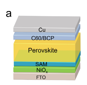
Experimental methods and research processFig.6a研究以Dual functional additive mercaptoacetamide(MAA
1. )As the core, a complete technical roadmap has been established from small area devices to large area modules, and theoretical calculations have been combined to deeply analyze the mechanism of action.Key material system: AdoptingFACsPerovskite system(FAIThePbI₂TheCsBr), MatchingC60Electronic transport layerpoly-4paczSelf assembling monolayers and innovative introductions
2. MAADual functional additive.
Process technology roadmap :lSubstrate processing and functional layer preparation:FTOAfter standard cleaning, the substrate is deposited in sequenceNiOxTunnel transport layer and
SAM interface layerlPreparation of perovskite layer: Different concentrationsMAAIntroducing precursor solution, using
Blade coating deposition method High quality thin films are formed through vacuum treatment and thermal annealinglDevice integrity: Preparation in sequencePEAIPassivation layerC₆₀/BCPElectronic Transport Layer andCu
3. Electrode.All processes, except for metal electrodes, are completed in an air environmentScale validationSuccessfully extended the process to5×5 cmand14×14 cmLarge area substrate, achieved through laser marking technology to interconnect sub cells in series, with module geometry filling factor reaching
4. 96%.Theoretical and Performance ValidationCombining density functional theory(DFT)Calculation Explanation
MAA
Defect suppression mechanism and long-term stability testing under photothermal and humid heat conditions to comprehensively verify the effectiveness of additives.Characterization methods and achievements
Quasi Fermi level splitting(QFLS)Quasi Fermi level splitting(QFLS)It is a key indicator for measuring the open circuit voltage potential of materials, and can also reveal the sources of non radiative recombination losses. This study investigates the photoluminescence quantum yield through photoluminescence(PLQY)Measure itquantitative evaluationMAA
Passivation effect on defects.The results show thatsutraMAAProcessed perovskite thin films, whichPLQYValue up to0.94%Significantly higher than the control group0.25%This indicates a significant reduction in non radiative recombination within the thin film, indicating device performance, especially open circuit voltage(VOC)The improvement. according toPLQYValue calculation,ΔQFLSincreased34.04 meVThis is related to the complete device

VOC
The increase is consistent with the magnitude.Figure 4g. PLQY values of the perovskite films without or with MAA deposited on glass substrates.Latest Release from Guangyan Technology
QFLS-MaperAnalyze the upper limit of material potential!Enlitech QFLS-MaperLet youCompetitive1/5cost advantageYou can obtain itQFLS MappingandQFLS
imaging
Clearly display the spatial distribution of quasi Fermi levels, making the quality of materials clear at a glance!Track our updates and get new technology information in real-time!J-VCurve measurement(current-
voltage curve)J-VThe curve is used for direct measurement of solar cells and modulesPhotoelectric conversion efficiency(PCE)Short circuit current density(Jsc)Open circuit voltage(Voc)And fill factor
(FF)
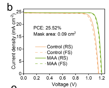
. Result: ◦Small area devices:OptimizedMAAProcessed small area perovskite solar cells (effective area)0.09 cm²), achieved25.52% PCEThe specific parameters areJsc 24.76 mA cm⁻²TheVoc 1.203 VandFF 85.68%In contrast, the control group devicesPCEfor23.46%Mainly due toVocandFFA significant decrease. In addition,MAAThe hysteresis index of the device(H-index)For0.63%
Significantly better than the control group 2.17% ◦Medium sized module:Expand the process to11.09 cm²The module, MAAThe processing module was implemented under reverse scanning22.87%ofPCE(Stable)PCEfor22.48%), itsVocfor5.952 VTheJsc 4.70 mA cm⁻²TheFF 81.75%And demonstrate good reproducibility. moduleH-indexfor1.48%The control group is
2.61% [S5] . ◦Large area module:In a larger area(113.00 cm²)On the module, MAAThe processed devices have also been realized20.18%of
PCE

.
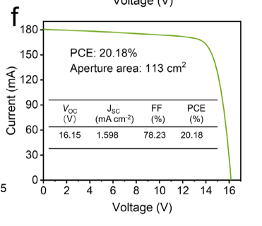
Figure 6b. J–V curves of the champion PSCs for the control and MAA
Figure 6c. I–V curves of champion PSMs without or with MAA modification (aperture area 11.09 cm2, 5 sub-cells)Figure 6f. I–V curves of champion PSMs with MAA modification (aperture area 113.00 cm2, 14 sub-cells)In the efficiency measurement of solar cells,EnliTechofSS-X AM1.5GStandard Spectral Solar SimulatorprovidedStable and preciseAM1.5G light source, itsA+Spectral gradeEnsure the development of new solar cells such as perovskite
/Accurate characterization of silicon stacked batteries.External quantum efficiency
(EQE)spectrumEQESpectral measurement is used forEvaluate the efficiency of the device in converting incident photons into electrons (current) under different wavelengths of illuminationIt can verifyJ-VMeasured results
JscValue and provide the response characteristics of the device in different spectral ranges.The results show that the device EQESpectral integrationJscvalue23.73 mA cm⁻², withJ-VThe measurement results are consistent.(
Figure S24)For the quantum efficiency analysis of solar cells,EnliTechofQE-RQuantum efficiency measurement systemIt's global1,000Multiple articles SCIThe choice of paper trust. It providesEQE/IQE/IPCE/SR testing capability, possessing300-2500 nmThe wide wavelength rangeandabove99.5%
The repeatability
.Other characterizations Analysis of Film Morphology and Crystal Structure(SEM, AFM, XRD, GIWAXS)evaluateMAAThe influence on the microstructure of perovskite thin films.MAAAfter introduction, the grain size changes from199 nmIncrease to386 nmThe roughness of the film decreases,(100)


The preferred orientation of crystal orientation is enhanced, and the residual tensile strain is significantly reduced.(Fig. 2a-i) Carrier Dynamics Analysis(PL, TRPL, FLIM)Evaluate the passivation effect and charge transfer characteristics of defects.MAAprocessedPLSignificant increase in intensity, carrier lifetime from366.9 nsextend to867.1 ns,FLIM
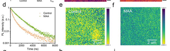
The electronic extraction efficiency of the display interface has been improved.(Fig. 4d-f) Band structure and surface potential(UPS, KPFM)analyzeMAAThe regulatory effect on energy level alignment.MAAProcessing causes the work function to shift upwards and the conduction band bottom to correspondingly shift upwards, resulting in a stronger appearance of the filmnType characteristics,KPFM

Displaying a more uniform surface potential distribution is beneficial for charge transfer.(Fig. 4a-c)Real time monitoring of crystallization kinetics(In situ optical microscope, in situPL)trackMAAThe regulatory mechanism of crystallization process.MAASignificantly delaying crystallization rate, expanding process window, during annealing processPL

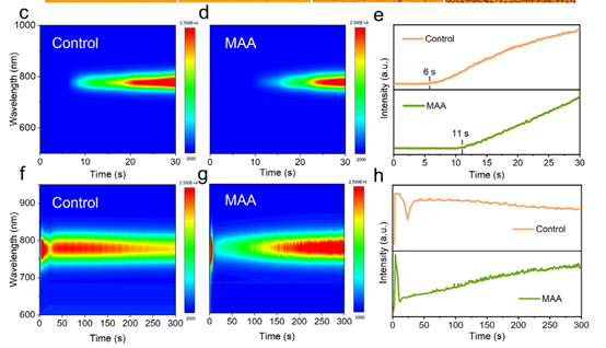
Continuous improvement in strength indicates improvement in film quality.(Fig. 3a-h) Theoretical calculation verification(DFT)clarifyMAAThe molecular mechanism of defect inhibition. The calculation results show thatMAAThe formation of vacancy defects after adsorption can be improved and effectively suppressedVPbTheVITheVFA
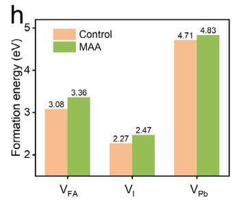
Waiting for defects to form.(Fig. 4h)Thermal stability and antioxidant activity(In-situ temperature variationXRD, mass spectrometry)evaluateMAAThe protective effect on material stability.MAAThe thermal decomposition temperature of thin films ranges from160°Cupgrade to180°C, with the ability to restoreI2forI⁻


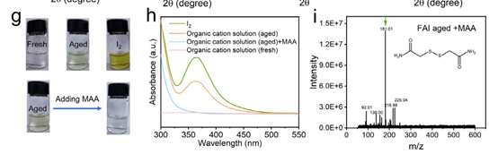
The ability to effectively inhibit precursor oxidation.(Fig. 5a-i)Long term operational stability(photothermal/ damp heat1120)Verify the durability of packaging components in practical application environments. Under photothermal conditionsMaintain after hours55094.5%Efficiency, under humid and hot conditionsMaintain after hours95.6%
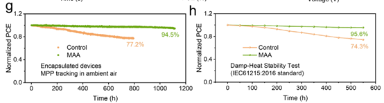
Efficiency.
(Fig. 6g-h)ConclusionThe research team has successfully developedMercaptoacetamide(MAA
)Dual functional additive strategy
1. Systematically solved the challenges of crystal control and environmental stability in the manufacturing of large-area perovskite solar modules.Core technological breakthrough:Optimization of Crystallization Dynamics:MAADelay the crystallization rate and expand the process window, with grain size ranging from199 nmSignificantly increased386 nm,
2. (100)The preferred orientation of crystal orientation is enhanced, and the residual strain is significantly reduced.Efficient defect passivationCarrier lifetime from366.9 nsextend to867.1 ns,PLQYfrom0.25%upgrade to0.94%,DFTCalculation verification
3. MAAEffectively suppress the formation of vacancy defects.Band Regulation and Charge Transport: Work function from-4.85 eVadjust to-4.64 eVPromote the upward movement of the conduction band bottom
4. nType features, more uniform surface potential distribution, and improved interface electron extraction efficiency.Enhanced environmental stability: Thermal decomposition temperature from160°Cupgrade to180°CAbove
5. MAA
The reducing properties effectively suppress precursor oxidation and enhance the intrinsic stability of the material.Device performance:small areaPSCachieve
25.52%high efficiency11.09 cm²Mini module implementation22.87% PCE(Stable efficiency)
22.48%)113.00 cm²
Large area modules achieve112020.18% PCEExcellent long-term stability performance: under photothermal conditionsMaintain after hours94.5%550efficiencyUnder humid and hot conditionsMaintain after hours
95.6%
efficiency