-
E-mail
info@phenom-china.com
-
Phone
18516656178
-
Address
Room T5705, Shanghai Hongqiao Libao Plaza, No. 88 Shenbin Road, Hongqiao Town, Minhang District, Shanghai
Funa Scientific Instruments (Shanghai) Co., Ltd
VSParticle invites you to meet at the 2nd International Conference on Artificial Intelligence Sensors and Transducers in Kuala Lumpur
Date: 2025-07-29Read: 1
INVITATION
The 2nd International Conference on Artificial Intelligence Sensors and Transducers will be held in Kuala Lumpur, Malaysia from July 29th to August 3rd. We sincerely invite you to attend and visit our booth [2] to interact and exchange ideas with technical sales engineer Vincent Mazzola and application expert Leandro Sacco, experience VSParticle's dry nano printing technology, and learn about its latest progress in gas sensing material research!
meeting timeFrom July 29th to August 3rd, 2025
venueMelia Hotel Kuala Lumpur, Malaysia
Booth Number:2

✨ Get a sneak peek at VSP exhibition highlights
Part 01.How can dry nano printing reshape the research and development path of sensing materials?
The metal oxide semiconductor (MOS) gas sensor technology based on MEMS has significant advantages over traditional monitoring methods: ppm level sensitivity, ability to detect multiple target gases, ease of miniaturization, strong scalability, and wide range. However, in terms of sensitivity and selectivity, existing MOS technologies are still unable to meet the needs of some application scenarios. By using the VSParticle P1 nano printing deposition system, the performance indicators of the sensor can be significantly improved: on the one hand, sensitivity can be increased by maximizing the specific surface area, and on the other hand, selective optimization can be achieved by precisely controlling the material composition.

The VSP-P1 nanoprinting deposition system provides a revolutionary solution for gas sensor manufacturing based on two core technologies: Spark Ablation and Inertial Impact Printing
-
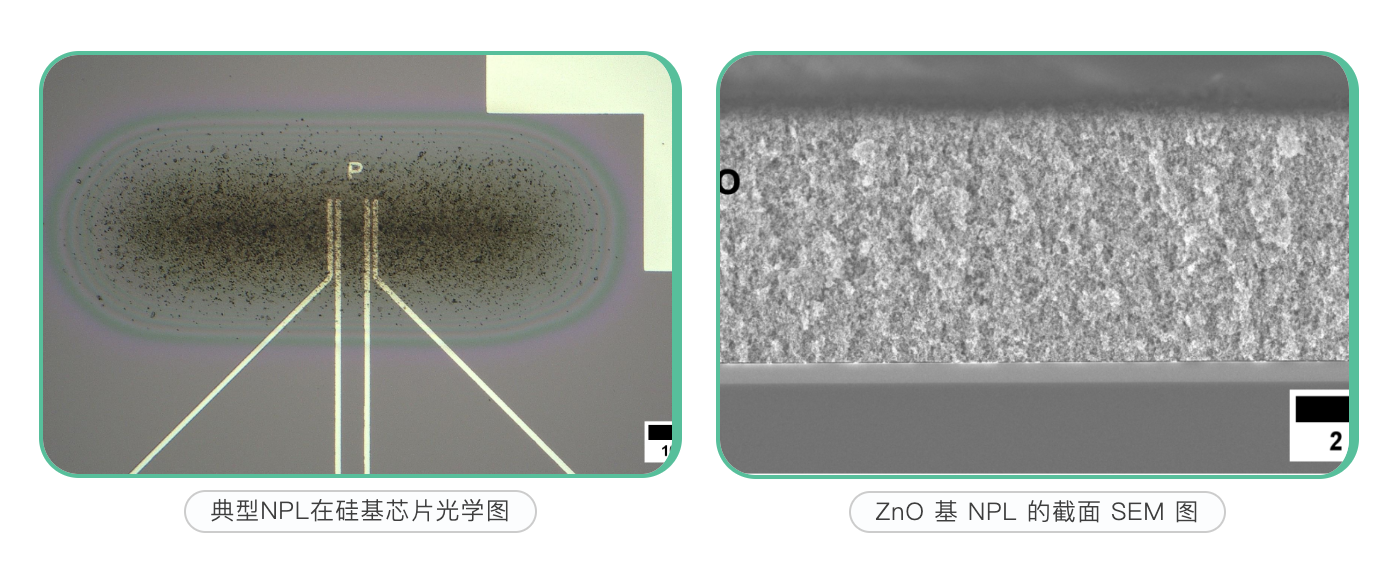
Spark erosionBy using high-voltage spark ablation to instantaneously vaporize metal electrodes, ultra pure nanoparticles (NPs) are generated, which can be flexibly mixed with metal oxides such as SnO ₂ NiO)、 Materials such as precious metal catalysts (such as Ag) enable customized nano porous layers (NPL).
Inertial impact printingHigh speed deposition of nanoparticles on sensor substrates can achieve patterned deposition without the need for photolithography or etching processes. The entire process avoids chemical pollution, ensures high purity and consistency of materials, and significantly improves sensor performance.
Part 02.High throughput, multi-component rapid screening of metal/oxide gas sensing coatings
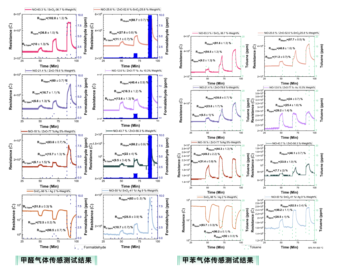
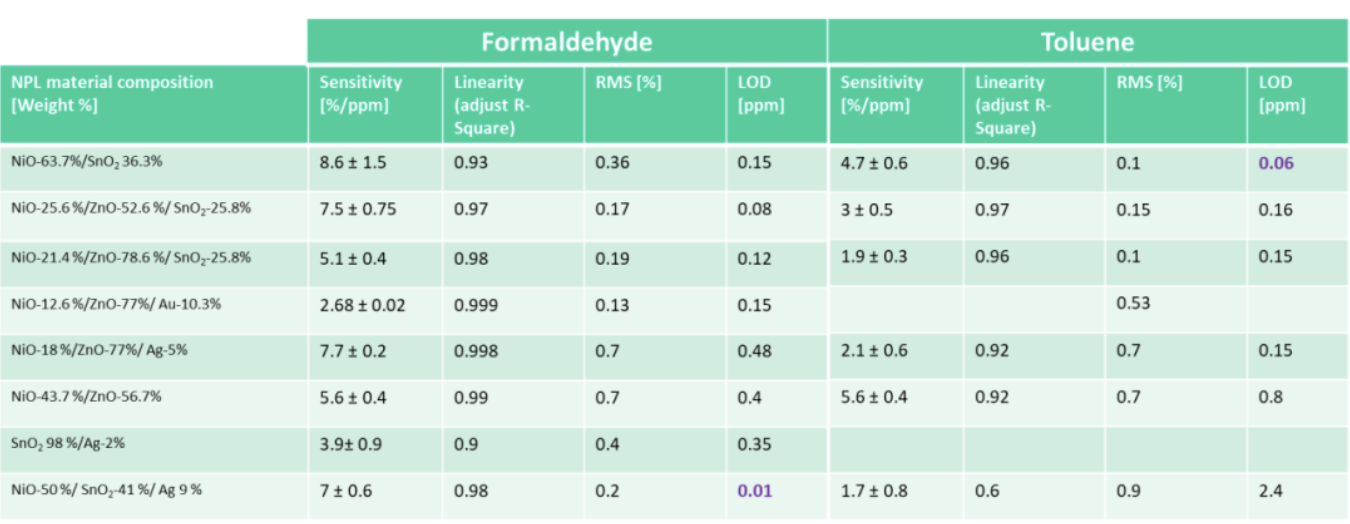
In this case, nano porous layers (NPLs) based on metal oxide semiconductors (MOS) and metal catalysts were deposited on a multi-sensor array platform by printing, and toluene and formaldehyde were used as target gases for testing. Up to three different components of NPLs are used as the sensing layer. Starting from key performance indicators such as sensitivity, selectivity, response/recovery time, and detection limit (LOD), the study systematically analyzed the influence of material composition on gas sensing performance.
Part 03.Nano porous gas sensing layer deposition service: rapidly creating high-performance sensing materials
To assist researchers and development teams in more efficiently advancing the material development and evaluation of gas sensors, VSParticle provides customized nano porous gas sensing layer deposition services, which can directly construct structurally controllable high-performance sensitive material layers on your target substrate. The services we can provide for you include:
Material customization and deposition
1. Use VSP spark ablation technology to generate 1-20nm particle size nanoparticles
2Optional single element materials (such as Pt, Pd, Au, Ni, etc.) can also be configured with multi-component or doped systems
3No dependence on solvents and ink, achieving maskless and dry printing
Controllable construction of nanostructures
1Form a high specific surface area, porous continuous network structure, optimize gas diffusion pathways and active reaction sites
2Key parameters such as sedimentation thickness, particle size distribution, sedimentation pattern/array design can be adjusted according to demand
3Provide single point, micro patterned array, and multi position comparative testing layout
Downstream adaptation and collaborative testing
1Can be deposited on various substrates, including MEMS chips, electrode structures, glass, silicon wafers, ceramics, etc
2Optional additional services: low-temperature heat treatment, conductivity testing, SEM morphology observation, spectral absorption, etc
.png)
If you are a researcher looking for more efficient gas sensing material development tools, an engineering expert focusing on batch processing and performance consistency of sensor arrays, or an industrial user seeking low-temperature compatibility and complex structure deposition solutions, welcome to VSParticle's booth to discuss face-to-face with us and explore the infinite possibilities of dry nano printing technology in AI gas sensing together!