-
E-mail
cindy_yst@instonetech.com
-
Phone
18600717106
-
Address
109-878, Building 20, No. 9 Antai Street, Konggang Street, Shunyi District, Beijing
Beijing Yingsitao Technology Co., Ltd
The darling of the research group - research specific desktop atomic layer deposition system (desktop ALD)
Date: 2025-08-18Read: 2
Anric TechnologiesEstablished in 2014, by renowned ALD process experts from Harvard UniversityProfessor Roy Gordon's GroupFounded by researchers with the aim of filling the market gapSmall desktop atomic layer depositionThe blank of ALD equipment provides design and optimization tools for universities, startups, companies exploring atomic layer deposition (ALD) technology, launching pilot production lines, and professional manufacturers.
The company focuses on the research of ALD processes and equipment, and its core technical members come from Harvard University. They have accumulated rich experience in ALD processes and can provide customers with customized solutions for complex processesSmall sample and low budget usersoption.
Introduction to Atomic Layer Deposition (ALD)
Atomic layer deposition is a special chemical vapor deposition technique that involves alternately introducing vapor precursors into a reaction chamber and generating gas-solid chemical reactions on the surface of the deposited substrate to form a thin film. ALD is usually composed of semi reactive sequences of A and B, with surface self confinement characteristics, excellent three-dimensional conformability, large-area uniformity, sub monolayer film thickness control, and low growth temperature.
Principle of Atomic Layer Deposition
The principle of ALD growth is to deposit thin films layer by layer on the substrate surface by alternately depositing precursor reactions.
An atomic layer deposition cycle can be divided into four steps:
1. Introducing the first precursor: Pulse the first precursor into the reaction chamber to undergo a chemical adsorption reaction with the substrate surface;
2. Inert gas cleaning: Clean the reaction chamber with an inert gas (such as nitrogen or gas) to remove the unreacted first precursor and by-products produced by the reaction;
3. Introducing the second precursor: Pulse the second precursor into the reaction chamber, causing it to undergo a chemical reaction with the first precursor adsorbed on the substrate surface to form a thin film;
4. Inert gas cleaning again: Use inert gas again to remove the unreacted second precursor and by-products.

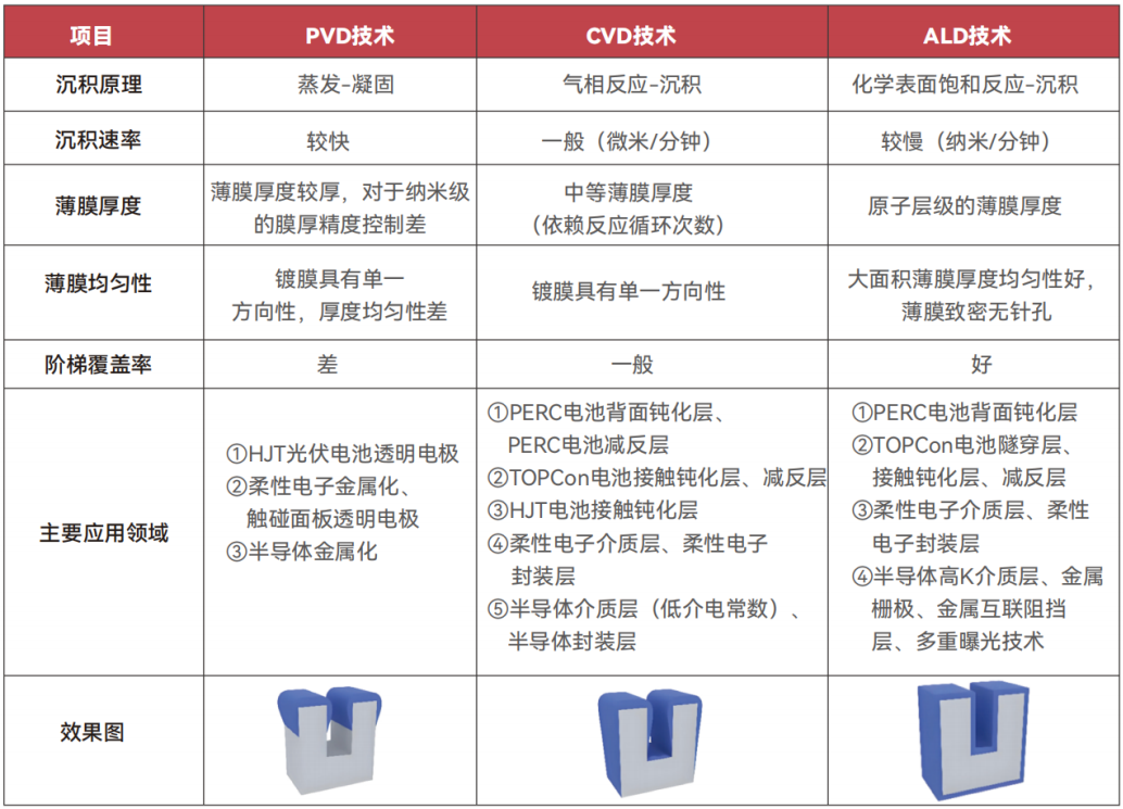
Comparison between ALD and other thin film deposition processes
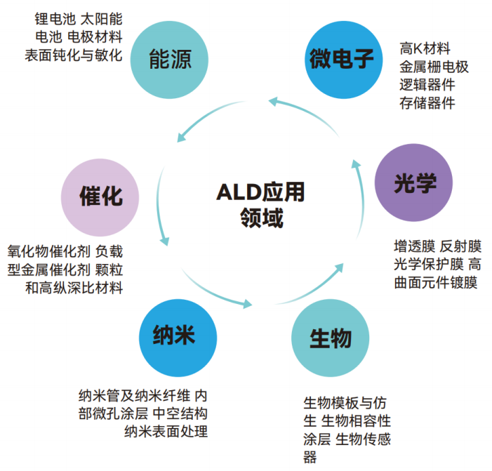
Application of ALD
Core advantages of the product
√ Can provide process support from experts in this field
√ Small and compact in size (occupying less space)
√ Low capacity chamber means rapid deposition and reduction of precursor waste, as well as deep penetration into three-dimensional structures
√ Rapid preheating (and cooling)
√ The distance between the precursor and the chamber is short (reducing the possibility of pipeline blockage)
AT 200M Thermal Atomic Layer Deposition
The smallest ALD in terms of volume on the market
ALD small enough to fit in a glove box
ALD that can be used as a powder

AT 200M Plus plasma enhancement+thermal atomic layer deposition


AT410/610/810 Hot Type


AT650P/850P (plasma enhanced) AT650T/850T (thermal type)


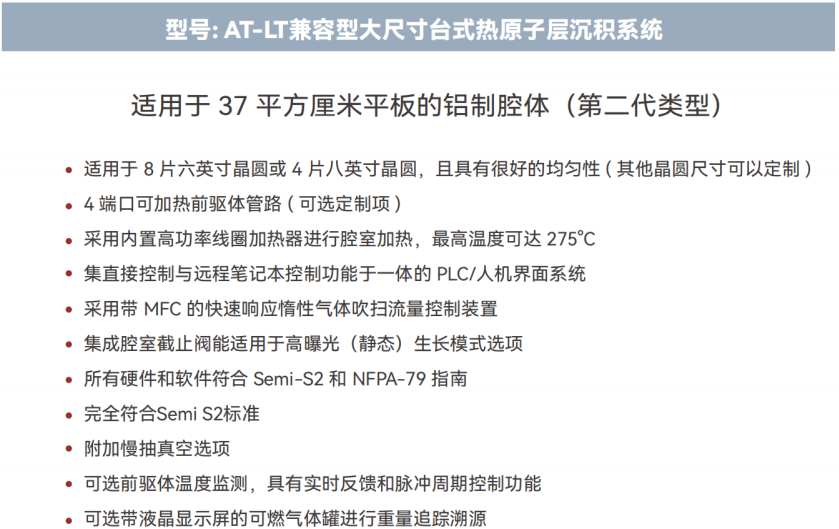
AT-LT Thermal Atomic Layer Deposition System

global100multipleCustomer repeat purchase | ||
serial number |
customer |
Application field |
1 |
Lam Research (6 units) |
|
2 |
Harvard University |
|
3 |
University of Helsinki |
Customers Mikko Ritala and Matti Putkonen |
4 |
Waseda University (multiple universities) |
Sensors, surface modification, nanoimprint lithography, advanced through-hole manufacturing (AlST) |
5 |
National Institute of Materials Science (NIMS) # 1 |
Phonons in surfaces and thin films, atomic scale low dimensional plasmonics, spin orbit splitting in nanomaterials |
6 |
National Institute of Materials Science (NIMS) # 2 |
Spin dependent transport in carbon nanotubes, nanogap fabrication and molecular transport, bandgap engineering in graphene, organic transistors |
7 |
The University of Tokyo |
ALD process |
8 |
The University of Tokyo |
Dr Onaya |
9 |
Oxford University (2 or more units) |
Customer Sebastian Bonilla |
10 |
Precision TEM Santa Clara, CA |
Sample preparation: HfO ₂, AlO ∝ |
11 |
Northwestern University (USA) |
|
12 |
Cambridge University (UK) |
|
13 |
Beijing Institute of Quantum Information Science |
|
14 |
ENS Paris (France, É cole Normale Sup é rieure) |
|
15 |
Rice University |
|
16 |
University of British Columbia (Canada) |
|
17 |
AMAT Applied Materials |
|
18 |
Private Company (Pivate Company) (Portland, Oregon, USA) 2 units |
TEM sample preparation: HfO ₂, AI ₂ O ∝, Ta ₂ O |
