- Phone
-
Address
2nd Floor, Building B, Jingang Technology Park, Qiaotou, Fuyong Street, Bao'an District, Shenzhen
Product Categories
- Fully automatic laser wafer marking machine
- Laser automation
- PCB Hard Board Precision Cutting Machine
- High precision marking and etching equipment
- Laser Welding Machine
- High precision laser cutting equipment
- Femtosecond laser cutting machine
- High precision laser marking machine
- Laser equipment accessories
- Fully automatic UV laser etching machine
- Picosecond laser cutting equipment
- Nanosecond laser cutting equipment
- High precision laser drilling equipment
- Femtosecond laser cutting equipment
- Fully automatic laser drilling micro hole equipment
Shenzhen Yunteng Laser Technology Co., Ltd
PERC cell laser marking machine
NegotiableUpdate on 02/08
- Model
- Nature of the Manufacturer
- Producers
- Product Category
- Place of Origin
Overview
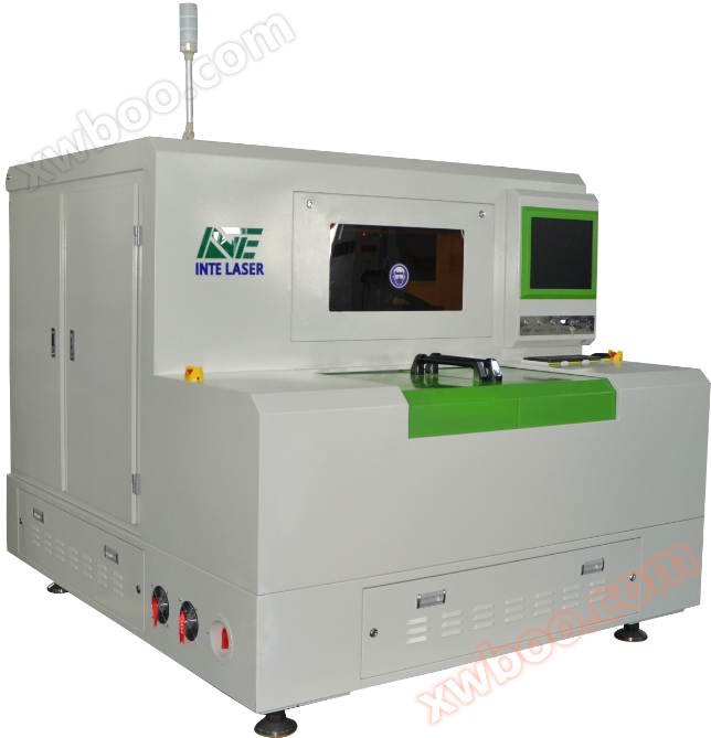
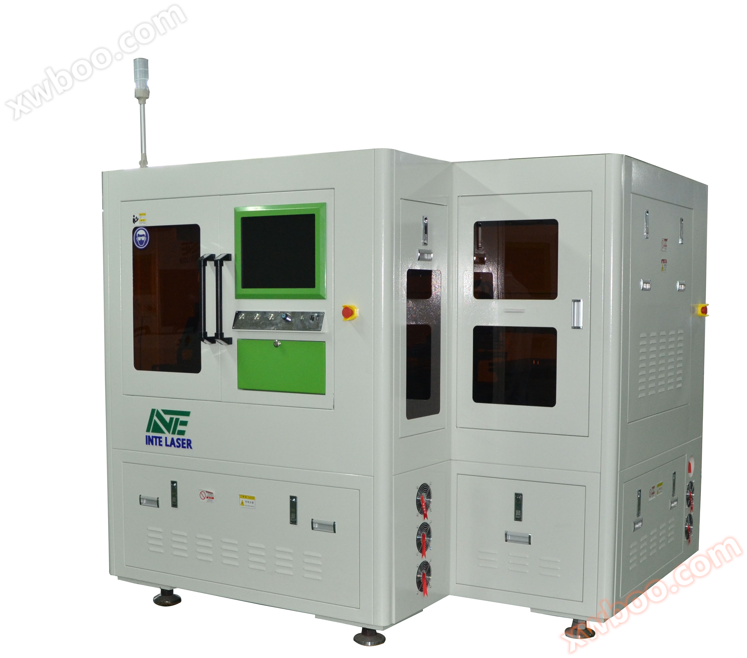
PERC cell laser marking machine
Product Details
Welcome to personalized customization
A professional customization team can provide personalized customization services according to the needs of customers. If you have such needs, please feel free to consult the customer service hotline: 13751030658.
Welcome to free sampling
Yunteng Laser can provide free sampling services. For technical consultation, process consultation, product consultation, and transportation consultation, please call directly!
Welcome to visit in person
Yunteng Laser's product quality is industry-leading. Welcome to visit and inspect the company on site! Multiple companies designated laser brands and witnessed together.
This device is mainly used for slotting the passivation layer on the back of PERC cells. Under special process conditions, the laser removes the passivation layer according to the drawing
Product features:
◆ Compact design structure to meet customer site requirements
◆ Stable laser source to meet long-term high-intensity operations
The INLINE process has a high degree of automation
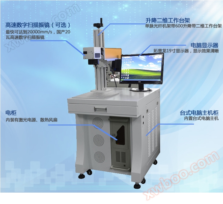
Technical parameters:
| ◆Project: | parameter | notes |
| ◆Silicon wafer size: | 156×156mm | Compatible with 125 × 125mm |
| ◆UPH: | ≥3600PCS | @1mm line spacing |
| ◆Uptime: | ≥95% | |
| ◆MTBF: | ≥250hours | |
| ◆MTTR : | ≤12hours | |
| ◆Yield: | ≥99.8% | |
| ◆Fragmentation rate: | ≤0.1% | |
| ◆Cutting accuracy: | ±0.3mm | |
| ◆cutting depth |
40μm±5μm |
customizable |
| ◆Other functions |
1. Can be used for the elimination of SiOx, ALOx, and SiNx film layers 2. Automatically identify fragments and unprocessed silicon wafers 3. Equipped with power monitoring device |
|
| ◆Equipment size |
2100mm×5500mm×1600mm |
▌Applying Materials
◆Crystalline silicon PERC cells (single crystal, polycrystalline)
◆Single crystal N-type battery
▌application area
◆Photovoltaic industry
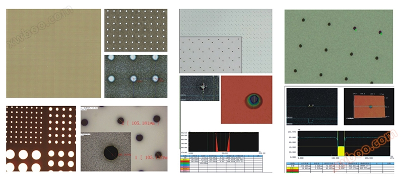
▌Example image of processing effect:

Why choose Yunteng Laser:
First class R&D team
85% of the company's employees have a college degree or above, and more than half of the total number of technical R&D personnel, among which R&D backbone personnel represent the top level in the industry.
Rich industry experience
Since its establishment in 2013, the company has gone through ups and downs, relying on first-class professional technology and strong research and development advantages, successfully providing laser equipment and application services to nearly 300 enterprises in different industries, and accumulating rich industry experience.
Integrated solution
The company has always adhered to the market-oriented approach and taken it as its responsibility to meet the actual needs of customers. Over the years, the company has independently developed and completed industry benchmark projects such as TP silver paste line+ITO automatic positioning etching system for touch screen industry, FPC+PCB high-precision automatic feeding and cutting system, laying a solid foundation for future development!
Focusing on professional cooperation and mutual benefit has been our driving force for many years!
Free solution design
Free sample evaluation
Free quotation consultation
Free trial of standard machines
Please consult relevant business personnel for details.

Similar Product Recommend