-
Phone
18017373226
-
Address
Room 703, South Building, Jinmao Garden, 2515 Pudong Avenue, Pudong New Area, Shanghai
Product Categories
Shanghai Pulangyuan Precision Electromechanical Co., Ltd

Lei chip measurement
NegotiableUpdate on 01/06
- Model
- Nature of the Manufacturer
- Producers
- Product Category
- Place of Origin
Overview
For customers and suppliers, surface texture is an extremely important parameter for determining the quality of epitaxial semiconductors
Product Details
Lei chip measurement
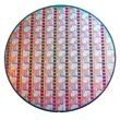
Due to the expanding applications of optoelectronic components in the fields of telecommunications and display technology, epitaxial technology has become a key technology for component production. Epitaxy refers to the process of depositing a very thin layer of semiconductor material on the surface of a single crystal substrate. Each crystal layer is called an epitaxial layer.
measurement
surface roughness
For customers and suppliers, surface texture is an extremely important parameter in determining the quality of epitaxial semiconductors. For current drivers, the roughness tolerance range has become narrower as the circuits printed on silicon wafers become smaller and smaller. The surface roughness of Lei chips is specified as nanometer level, so this requires the use of a system with very low noise and high resolution to measure Lei chips.


