-
E-mail
13967146609@126.com
-
Phone
13967146609
-
Address
3rd Floor, Building A, 3778 Jiangnan Avenue, Binjiang District, Hangzhou City, Zhejiang Province
Product Categories
Hangzhou Kefu Electromechanical Equipment Co., Ltd
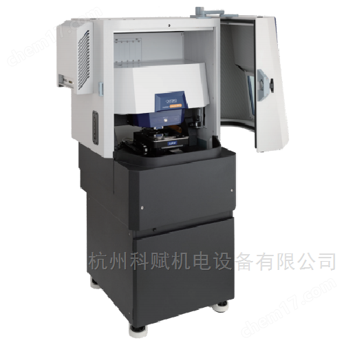

Jupiter Discovery Atomic Force Microscope
NegotiableUpdate on 01/22
- Model
- Nature of the Manufacturer
- Producers
- Product Category
- Place of Origin
Overview
Jupiter Discovery Atomic Force Microscopy (AFM) has significant advantages in performance and ease of operation. In the fields of scientific research and industrial applications, researchers generally pursue obtaining reliable detection data while simplifying operational processes. The current development of AFM technology has put forward higher requirements for measurement accuracy. Users need to achieve nanoscale detail observation and ensure the accuracy, stability, and detection efficiency of measurement results. Targeted optimization design of Jupiter Discovery, while maintaining high-performance detection capabilities, significantly improves the device's performance
Product Details
innovation AFM technology, large sample detection performance
lUltra high resolution imaging
lHigh throughput imaging
Optimize workflow and enhance user experience
lPre installed probes
lTop view and lateral dual view CCD system
lintelligent FFM Topography Mode
Rich accessories and strong scalability
lMultiple accessories to choose from
lExpand more features
Innovative design conceptSignificantly improve vertical and horizontal resolution
lAdopting optimized structural designEffectively improve system stiffness and reduce thermal drift effects, with noise levels below 25 pm.
lEquipped with excellent facilities LVDT position sensing technology significantly reduces system noise and maintains long-term stable high-resolution measurements, reducing the need for repeated calibration.
Obtain higher testing efficiency
lAdopting optimized electronic and mechanical bandwidth designThe scanning speed has been significantly improved compared to conventional large sample atomic force microscopes, while maintaining compatibility with various working modes and accessories.
lThe high-speed scanning function not only shortens the image acquisition timeIt also expands the application methods. This feature supports large-scale sample detection while maintaining high resolution, and can achieve complete characterization of larger samples through multi area stitching technology.
Simplified workflow
lAdopting pre installed probe designSimplify the probe replacement process.
lFully automated settings significantly reduce manual operation stepsSimply click the mouse to complete parameter optimization.
lEquipped with a multi angle optical observation systemIncluding two sets of CCD systems for side view observation and high-definition top view, it helps to quickly locate the detection area.
Easy to operateHigh usability
lIntelligent workflowAutomatically optimize parameter settings and data collection
lAll operating modes follow a unified design philosophy and guide users through automated processes to complete configurations. The system achieves full process automation within the technically feasible range, and for links that require manual interventionProvide detailed operational assistance to ensure that the operator completes the operation smoothly.
AutoPilot intelligent algorithm improves operational efficiency
lThe AutoPolit feature focuses on optimizing the basic imaging of the tap mode and the new FFM Topography mode, while other advanced modes have also been greatly simplified. Even more advanced modes such as Conductive Atomic Force Microscopy (CAFM), Kelvin Probe Microscopy (KPFM), Piezoelectric Force Microscopy (PFM), and Scanning Capacitive Microscopy (SCM) can now be easily used without extensive experience.
Automated multi-point repeatability detection process
lAutomated testing module, supporting users to configure differentiated scanning schemes at preset sample coordinate positions, suitable for industrial quality inspection field(QA/QC), Including quality monitoring of wafer surface deposition/etching processes and analysis of surface morphology characteristics. Simultaneously supporting the automation of repetitive experimental processes in scientific research scenarios, coupled with high-speed scanning technology, it can be extended to systematic detection of large-sized samples.
Similar Product Recommend


