04,28,2026 80 views
ASMPT has a presence in over 30 countries, and the group continues to leverage its advantages in business networks and resources to drive the growth of its main business - the Post Process Equipment, Materials, and SMT Solutions business units.
Post process equipment business

Material business
SMT Solution Business
Established in Hong Kong in 1975, the group is an equipment that provides technology and solutions for all process steps in semiconductor packaging and electronic product production, including semiconductor packaging materials and back-end (chip integration, soldering, packaging) to SMT processes.
No other equipment supplier has a similar product portfolio and extensive knowledge and experience in assembly and SMT procedures.
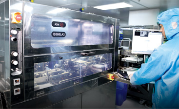
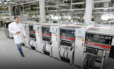
Production and provision of semiconductor embedding and packaging equipment for the post-processing equipment business, applied in the microelectronics, semiconductor, optoelectronics, and optoelectronic markets. It provides diversified products such as solid crystal systems, wire bonding systems, and dropper systems,
Cutting and forming system and production line equipment. The material business produces and provides semiconductor packaging materials, consisting of lead frame parts and molded interconnect substrate parts. The SMT solution business is responsible for SMT
Development and distribution of DEK printing machines for the semiconductor and solar markets, as well as SIPLACE SMT mounting solutions.
ASMPT is headquartered in Singapore and has been listed on the Hong Kong Stock Exchange since 1989.
The samples tested by ASMPT company this time are very special, measuring the surface tension of some photoresists and the contact angle of wafers. There are high requirements for the contact angle testing instrument itself and software analysis capabilities.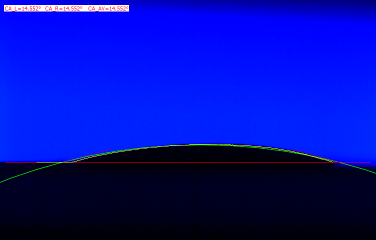
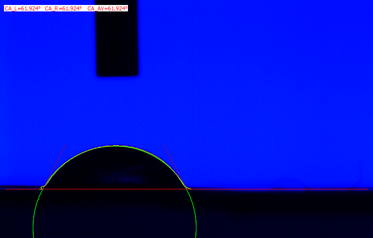
Shanghai Solon, as a strategic investment company in the American Kono Asia region, has independent research and development capabilities as well as processing and production capabilities. The contact angle measurement algorithm used is the Asha algorithm, and the Equation of State algorithm proposed by Professor A.W. Neumann is employed,
Calculate and analyze the surface tension value of the photoresist and its corresponding contact angle value. Thus providing users with a comprehensive solution for the application of surface chemistry in actual wafers and chips.
We are willing to share with more users the interface chemical measurement technology and application solutions of Shanghai Solon and American Kono. We provide measurement solutions that are suitable for you.