-
E-mail
info@chip-nova.com
-
Phone
15860798525
-
Address
Room 206, North Building, Weiye Building, Innovation and Entrepreneurship Park, No.11 Huoju East Road, Huli District, Xiamen City, Fujian Province
Xiamen Chaoxinxin Technology Co., Ltd
Conference Invitation | Chaoxin Technology cordially invites you to attend the 2025 National Electronic Microscopy Academic Annual Conference
Date: 2025-09-19Read: 56
The 2025 National Conference on Electron Microscopy will be held from September 26th to 30th at the Wuhan International Conference Center.
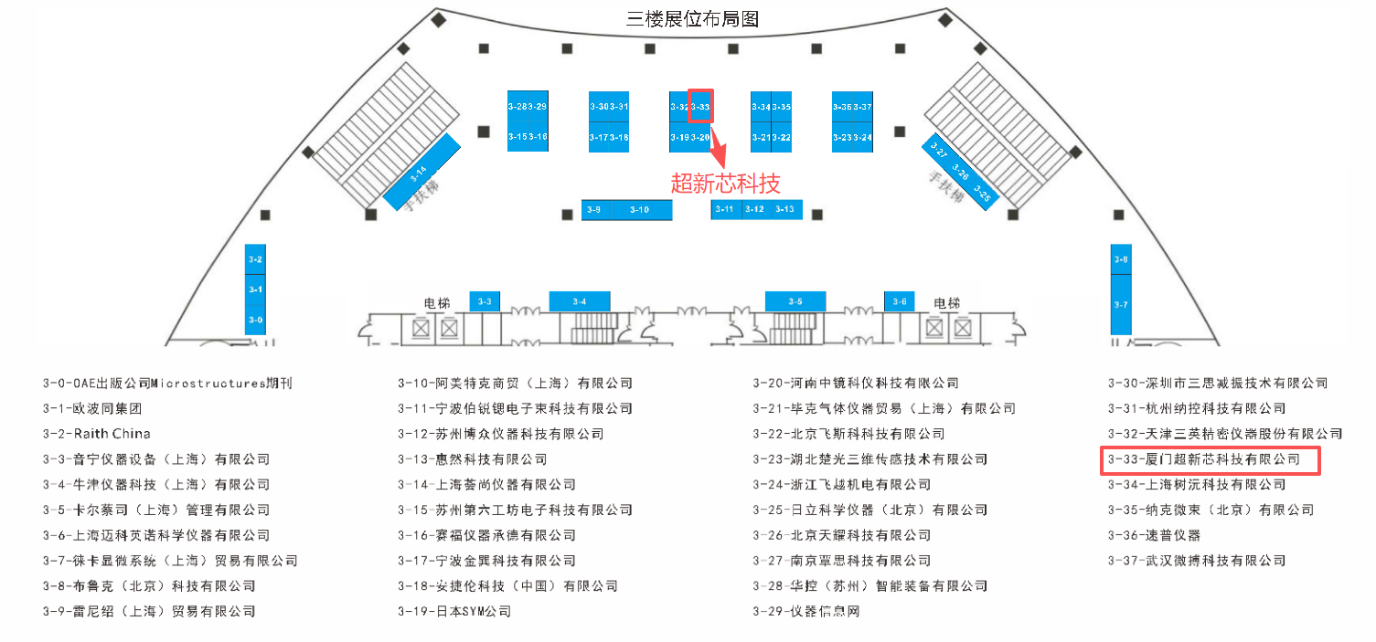
As an industry leader in in-situ electron microscopy solutions, Chaoxin Technology will showcase its in-situ electron microscopy technology at the conference, booth number 3-33. We will provide professional consultation and technical support on-site, and even offer exquisite gifts for you to collect! We sincerely invite experts, scholars, scientific and technological personnel, and young students from universities, research institutes, related industries from all over the country to visit our booth!
01 Meeting Information
The academic exchange content of this annual conference includes: aberration corrected transmission electron microscopy, in-situ microscopy techniques (including mechanics, physics, chemistry, biology, etc.), high-resolution scanning electron microscopy, microbeam analysis, scanning probe microscopy (including STM, AFM, etc.), low-temperature electron microscopy, and laser confocal microscopy. The conference also includes the basic research and application achievements of these technologies in cutting-edge disciplines such as physics, chemistry, geology, life sciences, medicine, and information science, as well as in new energy technology, thermoelectric materials, information technology, environmental science and technology, advanced structural materials, and other fields; The conference will showcase the latest developments in microscopy related theories, instrument manufacturing, technology, and experimental methods; The conference will promote the operation, management, maintenance, and open sharing of electron microscopes and other microscopy instruments, as well as exchange on the construction and development of experimental platforms;
Meeting time and location
Date: September 26-30, 2025 (reported on the 26th)
Location: Wuhan International Convention Center
Booth Number: 3-33
conference organizer
Editorial Department of Journal of Electron Microscopy, Chinese Society for Electron Microscopy (International)
Special sub venue
1) Microscopy theory, instrument methods and techniques;
2) In situ electron microscopy characterization;
3) Characterization of microstructure of functional materials;
4) Structural materials and defects, interfaces, surfaces, phase transitions and diffusion;
5) The application of advanced microscopic analysis technology in industrial materials;
6) Scanning probe microscopy characterization (STM/AFM, etc.);
7) Characterization of material microstructure using electron diffraction and electron microscopy holography (including SEM, EBSD, and TEM);
8) The application of focused ion beam (FIB) in materials science;
9) Low temperature electron microscopy characterization;
10) Development and application of biomedical electron microscopy technology;
11) The application of microscopy in the fields of agriculture, forestry, and biological sciences (such as super-resolution microscopy, confocal laser microscopy, etc.);
12) Research and application of agricultural and forestry electron microscopy;
13) Advanced material microscopic characterization and cutting-edge innovation;
14) Microscopic scientific instruments and material microstructure processing technology;
15) Intelligent upgrade and open sharing of microscopy platform.
02 About Super New Chip
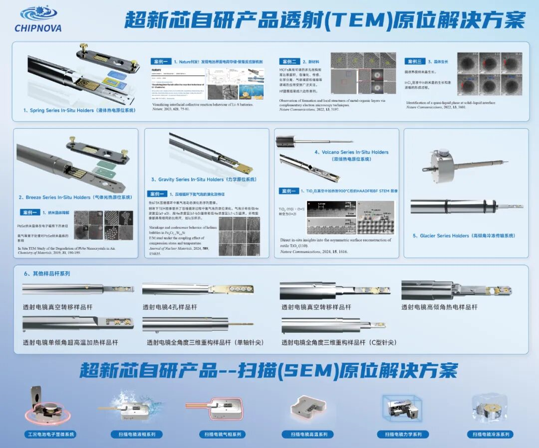
CHIPNOVA, as an early pioneer in in-situ chip technology, was founded by a senior team in the industry and has been deeply involved in MEMS chip manufacturing and in-situ electron microscopy technology for more than ten years. It maintains long-term close cooperation with top universities and research institutions such as the University of California, Berkeley and Xiamen University to explore the future applications of in-situ technology. At present, the company has been awarded honorary titles such as National High tech Enterprise, Specialized and Innovative Enterprise, and "Gazelle" Enterprise.
Core advantages: MEMS chip design and processing technology with core intellectual property rights, independently developed in-situ electron microscopy software and hardware systems, professional in-situ electron microscopy application team, and accumulated rich in-situ electron microscopy technology application cases.
Our clients have covered renowned research institutions and major universities worldwide, and our professional in situ electron microscopy solutions have helped our clients publish over 100 papers in various journals (including CNS top journals). Chaoxinxin will continue to be driven by innovation, empowering scientific research and industry, and helping China's high-precision instruments and in-situ analysis technology move towards the forefront of the world!
01
Product Display and Customer Cases
CHIPNOVA (Super New Chip Technology)
Address: Room 206, North Building, Weiye Building, Innovation and Entrepreneurship Park, No. 11 Huoju East Road, Huli District, Xiamen City, Fujian Province